
6.12: Band Diagrams, Semiconductors, and Doping
- Page ID
- 408822
\( \newcommand{\vecs}[1]{\overset { \scriptstyle \rightharpoonup} {\mathbf{#1}} } \)
\( \newcommand{\vecd}[1]{\overset{-\!-\!\rightharpoonup}{\vphantom{a}\smash {#1}}} \)
\( \newcommand{\id}{\mathrm{id}}\) \( \newcommand{\Span}{\mathrm{span}}\)
( \newcommand{\kernel}{\mathrm{null}\,}\) \( \newcommand{\range}{\mathrm{range}\,}\)
\( \newcommand{\RealPart}{\mathrm{Re}}\) \( \newcommand{\ImaginaryPart}{\mathrm{Im}}\)
\( \newcommand{\Argument}{\mathrm{Arg}}\) \( \newcommand{\norm}[1]{\| #1 \|}\)
\( \newcommand{\inner}[2]{\langle #1, #2 \rangle}\)
\( \newcommand{\Span}{\mathrm{span}}\)
\( \newcommand{\id}{\mathrm{id}}\)
\( \newcommand{\Span}{\mathrm{span}}\)
\( \newcommand{\kernel}{\mathrm{null}\,}\)
\( \newcommand{\range}{\mathrm{range}\,}\)
\( \newcommand{\RealPart}{\mathrm{Re}}\)
\( \newcommand{\ImaginaryPart}{\mathrm{Im}}\)
\( \newcommand{\Argument}{\mathrm{Arg}}\)
\( \newcommand{\norm}[1]{\| #1 \|}\)
\( \newcommand{\inner}[2]{\langle #1, #2 \rangle}\)
\( \newcommand{\Span}{\mathrm{span}}\) \( \newcommand{\AA}{\unicode[.8,0]{x212B}}\)
\( \newcommand{\vectorA}[1]{\vec{#1}} % arrow\)
\( \newcommand{\vectorAt}[1]{\vec{\text{#1}}} % arrow\)
\( \newcommand{\vectorB}[1]{\overset { \scriptstyle \rightharpoonup} {\mathbf{#1}} } \)
\( \newcommand{\vectorC}[1]{\textbf{#1}} \)
\( \newcommand{\vectorD}[1]{\overrightarrow{#1}} \)
\( \newcommand{\vectorDt}[1]{\overrightarrow{\text{#1}}} \)
\( \newcommand{\vectE}[1]{\overset{-\!-\!\rightharpoonup}{\vphantom{a}\smash{\mathbf {#1}}}} \)
\( \newcommand{\vecs}[1]{\overset { \scriptstyle \rightharpoonup} {\mathbf{#1}} } \)
\( \newcommand{\vecd}[1]{\overset{-\!-\!\rightharpoonup}{\vphantom{a}\smash {#1}}} \)
\(\newcommand{\avec}{\mathbf a}\) \(\newcommand{\bvec}{\mathbf b}\) \(\newcommand{\cvec}{\mathbf c}\) \(\newcommand{\dvec}{\mathbf d}\) \(\newcommand{\dtil}{\widetilde{\mathbf d}}\) \(\newcommand{\evec}{\mathbf e}\) \(\newcommand{\fvec}{\mathbf f}\) \(\newcommand{\nvec}{\mathbf n}\) \(\newcommand{\pvec}{\mathbf p}\) \(\newcommand{\qvec}{\mathbf q}\) \(\newcommand{\svec}{\mathbf s}\) \(\newcommand{\tvec}{\mathbf t}\) \(\newcommand{\uvec}{\mathbf u}\) \(\newcommand{\vvec}{\mathbf v}\) \(\newcommand{\wvec}{\mathbf w}\) \(\newcommand{\xvec}{\mathbf x}\) \(\newcommand{\yvec}{\mathbf y}\) \(\newcommand{\zvec}{\mathbf z}\) \(\newcommand{\rvec}{\mathbf r}\) \(\newcommand{\mvec}{\mathbf m}\) \(\newcommand{\zerovec}{\mathbf 0}\) \(\newcommand{\onevec}{\mathbf 1}\) \(\newcommand{\real}{\mathbb R}\) \(\newcommand{\twovec}[2]{\left[\begin{array}{r}#1 \\ #2 \end{array}\right]}\) \(\newcommand{\ctwovec}[2]{\left[\begin{array}{c}#1 \\ #2 \end{array}\right]}\) \(\newcommand{\threevec}[3]{\left[\begin{array}{r}#1 \\ #2 \\ #3 \end{array}\right]}\) \(\newcommand{\cthreevec}[3]{\left[\begin{array}{c}#1 \\ #2 \\ #3 \end{array}\right]}\) \(\newcommand{\fourvec}[4]{\left[\begin{array}{r}#1 \\ #2 \\ #3 \\ #4 \end{array}\right]}\) \(\newcommand{\cfourvec}[4]{\left[\begin{array}{c}#1 \\ #2 \\ #3 \\ #4 \end{array}\right]}\) \(\newcommand{\fivevec}[5]{\left[\begin{array}{r}#1 \\ #2 \\ #3 \\ #4 \\ #5 \\ \end{array}\right]}\) \(\newcommand{\cfivevec}[5]{\left[\begin{array}{c}#1 \\ #2 \\ #3 \\ #4 \\ #5 \\ \end{array}\right]}\) \(\newcommand{\mattwo}[4]{\left[\begin{array}{rr}#1 \amp #2 \\ #3 \amp #4 \\ \end{array}\right]}\) \(\newcommand{\laspan}[1]{\text{Span}\{#1\}}\) \(\newcommand{\bcal}{\cal B}\) \(\newcommand{\ccal}{\cal C}\) \(\newcommand{\scal}{\cal S}\) \(\newcommand{\wcal}{\cal W}\) \(\newcommand{\ecal}{\cal E}\) \(\newcommand{\coords}[2]{\left\{#1\right\}_{#2}}\) \(\newcommand{\gray}[1]{\color{gray}{#1}}\) \(\newcommand{\lgray}[1]{\color{lightgray}{#1}}\) \(\newcommand{\rank}{\operatorname{rank}}\) \(\newcommand{\row}{\text{Row}}\) \(\newcommand{\col}{\text{Col}}\) \(\renewcommand{\row}{\text{Row}}\) \(\newcommand{\nul}{\text{Nul}}\) \(\newcommand{\var}{\text{Var}}\) \(\newcommand{\corr}{\text{corr}}\) \(\newcommand{\len}[1]{\left|#1\right|}\) \(\newcommand{\bbar}{\overline{\bvec}}\) \(\newcommand{\bhat}{\widehat{\bvec}}\) \(\newcommand{\bperp}{\bvec^\perp}\) \(\newcommand{\xhat}{\widehat{\xvec}}\) \(\newcommand{\vhat}{\widehat{\vvec}}\) \(\newcommand{\uhat}{\widehat{\uvec}}\) \(\newcommand{\what}{\widehat{\wvec}}\) \(\newcommand{\Sighat}{\widehat{\Sigma}}\) \(\newcommand{\lt}{<}\) \(\newcommand{\gt}{>}\) \(\newcommand{\amp}{&}\) \(\definecolor{fillinmathshade}{gray}{0.9}\)Band diagrams
As we saw for hydrogen in lecture, band diagrams can be thought of as the continuum limit of MO theory, allowing us to think about a long chain of bonds (or even a crystalline solid!) instead of just a dimer. To recap, let's imagine what building up a carbon solid - diamond- would be like. Start with just a few carbon atoms: with electronic configuration \(1 \mathrm{~s}^2 2 \mathrm{~s}^2 2 \mathrm{p}^2\), they each bring 6 electrons, including two core electrons and four valence electrons. Remember - the core electrons live closest to the nucleus; they require the most energy to remove. The valence electrons live further away from the nucleus: these are the electrons that participate in bonding. Now, let's bring in some more atoms.
We know from previous weeks that carbon can form \(\mathrm{sp}^3\) hybridized bonds - these are tetrahedral, so every carbon is coordinated to bond with four other neighboring carbon atoms. The bonding happens between (hybridized) valence electrons: if we were working at \(0 \mathrm{~K}\) - absolute zero temperature - we could imagine a rigid structure of nuclei and bonds. And remember, a diamond could have moles of electrons, meaning moles of bonds! The \(\mathrm{sp}^3\) hybridized valence electrons collectively form the valence band. Unlike a MO diagram, in which we drew one energy level for each type of bonding and antibonding orbital, the moles of electrons in a solid form distributions: all of the 1s electrons are distributed around a very low energy value, for example.
But what happens if we turn up the temperature? It turns out, several interesting things: for one, the thermal energy now available to the system allows for atoms to begin vibrating. Though the core electrons are too low in energy to be affected, some of the electrons in the tail of the valence band gain enough energy that they can delocalize (think back to our ionization days!), and become conducting electrons. The electrons that have been excited form the conduction band.
In a metal, it requires little thermal energy to excite a sea of electrons that readily carry charge (current). It happens at room temperature! This can occur in two ways: either a band is only partially full, so there are lots of states nearby in energy to be populated, or a full band overlaps with an empty band, so again it's easy for the electrons to hop between. In a semiconductor, the energy gap between the full valence band and the empty (at \(0 \mathrm{~K}\) ) conduction band is a little bit larger: as the temperature increases, statistically, a few electrons gain enough energy to hop across the gap and conduct. Finally, in an insulator, the space between the highest full band and the lowest energy band is very large: it takes so much energy for an electron to jump to the conduction band that it doesn't happen under normal temperature and operating conditions.

Semiconductors
Semiconductors are defined by their name: they are kinda conductive. These materials have a band gap, but it’s not as big as that of an insulator. Often in the field, \(3 \mathrm{~eV}\) serves as a rough cut-off: band gaps below this energy belong to semiconductors, while higher energy systems are considered insulating. Silicon is by far the most mature semiconductor technology: it is used in all sorts of applications and devices.
Semiconductors have a particularly interesting property that make them useful: they can function as transducors between electricity and light. If you shine light with sufficient energy on an semiconductor, it excites carriers inside the material: specifically, one photon excites an electron from the valance band up to the conduction band, where it is mobile. What happens to the atom that electron came from? It has essentially become electron-deficient, or ionized: it can be thought of as an extra positive charge in the valence band called a hole. Similar to electrons in the conduction band, holes in the valence band can move around: both carriers play a role in how conductive a material is! This is the operating principle of a solar cell: light shines on a material, and is converted into electricity. And what sets the relevant energy scale? The band gap, of course! Light with energy greater than the bandgap will be absorbed by the semiconductor and create carriers; light lower in energy than the bandgap will not be absorbed and will have no effect.
Similarly, semiconductors can transduce electricity to light as well: think of an LED! LEDs require a little more thought (and engineering) because while it’s easy for a passing photon to find an electron/hole pair to excite, it’s not quite as simple to bump an electron and a hole together so they recombine and emit light. The device used to engineer this process is called a PN junction.
Doping
Though we won't cover PN junction operation in \(3.091\), we will talk about the ingredients to make one. A PN junction is formed by stacking a \(\mathrm{p}\)-type semiconductor next to an \(\mathrm{n}\)-type semiconductor material. A \(p-type\) semiconductor contains extra holes, while an \(n-type\) semiconductor contains extra electrons. You may be wondering, extra carriers compared to what? A plain semiconductor material - a single material (like \(\mathrm{Si}\)) or an alloy (like \(\mathrm{GaAs}\) - is called intrinsic. The extra carriers are introduced via doping: adding a small fraction of a different type of atom to introduce new carriers. \(\mathrm{P}\)-type materials are obtained by doping with atoms with fewer electrons: think doping a group IV semiconductor with group III atoms. \(\mathrm{N}\)-type materials are obtained by doping with atoms with more electrons: think doping group IV with group V.
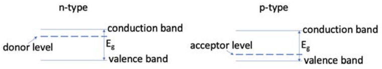
The extra carriers don't have quite the same energy structures as the lattice they are substituting into. Consider adding \(\mathrm{P}\) into \(\mathrm{Si}\). \(\mathrm{P}\) has 5 valence electrons, compared to 4 in a \(\mathrm{Si}\) atom. Remember that the electronic bands in a material are really an extension of their MO diagrams: adding just one electron to an MO diagram had a drastic effect on the bonding! In the local environment of the \(\mathrm{n}\)-type dopant, there is one too many electrons. This electron is much higher in energy than the other valence electrons: it forms a donor level within the band gap. The donor levels are often so close to the conduction band that thermal energy is enough to excite the extra carriers into the conduction band. Therefore, in \(\mathrm{n}\)-type materials, the extra carriers are electron donors.
Now, consider adding \(\mathrm{Ga}\) into \(\mathrm{Si}\). \(\mathrm{Ga}\) is missing an electron compared to \(\mathrm{Si}\), so it creates an extra hole in the conduction band. Energetically, things would be much more favorable if there were an electron populating that site: the hole creates an acceptor level close to the valence band. The holes are readily excited to the valence band, where they conduct. In both of these processes, the band gap itself is unaffected by the doping: rather, the extra states within the band gap increase the carrier population at thermal equilibrium.
Example: If you dope 1 cubic meter of \(\mathrm{Ge}\) with \(2.43 \mathrm{mg} \mathrm{Mg}\), how many carriers does each substitution yield and how many carriers are generated? What kind of doping is this?
- Answer
-
We can determine how many carriers each substitution yields using the periodic table: \(\mathrm{Ge}\) is group IV, while \(\mathrm{Mg}\) is group II. Therefore, \(\mathrm{Ge}\) has four valence electrons compared to \(\mathrm{Mg}\)'s two. Each substitution generates 2 extra carriers. Additionally, because we are doping with an electron-deficient material, this is \(\mathrm{p}\)-type doping. Finally, let's set up the unit conversion to determine how many carriers are created:
\[2.43 \mathrm{mg} \mathrm{Mg} \times\left(\dfrac{10^{-3} \mathrm{~g}}{1 \mathrm{mg}}\right)\left(\dfrac{1 \mathrm{~mol} \mathrm{Mg}}{24.3 \mathrm{~g} \mathrm{Mg}}\right)=10^{-4} \mathrm{~mol} \mathrm{Mg} \nonumber\]
Then, since each \(\mathrm{Mg}\) provides two holes:
\[\dfrac{2 \text { holes }}{\text { Mg substitution }} \times 10^{-4} \mathrm{~mol} \mathrm{Mg}=2 \times 10^{-4} \mathrm{~mol} \text { holes } \nonumber\]
Finally, we can pull out Avogadro:
\[\left(2 \times 10^{-4} \mathrm{~mol} \text { holes }\right)\left(6.602 \times 10^{23} \dfrac{\text { holes }}{\text { mol holes }}\right)=1.32 \times 10^{20} \text { holes } \nonumber\]