8.3: Scanning Tunneling Microscopy
- Page ID
- 55919

\( \newcommand{\vecs}[1]{\overset { \scriptstyle \rightharpoonup} {\mathbf{#1}} } \)
\( \newcommand{\vecd}[1]{\overset{-\!-\!\rightharpoonup}{\vphantom{a}\smash {#1}}} \)
\( \newcommand{\id}{\mathrm{id}}\) \( \newcommand{\Span}{\mathrm{span}}\)
( \newcommand{\kernel}{\mathrm{null}\,}\) \( \newcommand{\range}{\mathrm{range}\,}\)
\( \newcommand{\RealPart}{\mathrm{Re}}\) \( \newcommand{\ImaginaryPart}{\mathrm{Im}}\)
\( \newcommand{\Argument}{\mathrm{Arg}}\) \( \newcommand{\norm}[1]{\| #1 \|}\)
\( \newcommand{\inner}[2]{\langle #1, #2 \rangle}\)
\( \newcommand{\Span}{\mathrm{span}}\)
\( \newcommand{\id}{\mathrm{id}}\)
\( \newcommand{\Span}{\mathrm{span}}\)
\( \newcommand{\kernel}{\mathrm{null}\,}\)
\( \newcommand{\range}{\mathrm{range}\,}\)
\( \newcommand{\RealPart}{\mathrm{Re}}\)
\( \newcommand{\ImaginaryPart}{\mathrm{Im}}\)
\( \newcommand{\Argument}{\mathrm{Arg}}\)
\( \newcommand{\norm}[1]{\| #1 \|}\)
\( \newcommand{\inner}[2]{\langle #1, #2 \rangle}\)
\( \newcommand{\Span}{\mathrm{span}}\) \( \newcommand{\AA}{\unicode[.8,0]{x212B}}\)
\( \newcommand{\vectorA}[1]{\vec{#1}} % arrow\)
\( \newcommand{\vectorAt}[1]{\vec{\text{#1}}} % arrow\)
\( \newcommand{\vectorB}[1]{\overset { \scriptstyle \rightharpoonup} {\mathbf{#1}} } \)
\( \newcommand{\vectorC}[1]{\textbf{#1}} \)
\( \newcommand{\vectorD}[1]{\overrightarrow{#1}} \)
\( \newcommand{\vectorDt}[1]{\overrightarrow{\text{#1}}} \)
\( \newcommand{\vectE}[1]{\overset{-\!-\!\rightharpoonup}{\vphantom{a}\smash{\mathbf {#1}}}} \)
\( \newcommand{\vecs}[1]{\overset { \scriptstyle \rightharpoonup} {\mathbf{#1}} } \)
\( \newcommand{\vecd}[1]{\overset{-\!-\!\rightharpoonup}{\vphantom{a}\smash {#1}}} \)
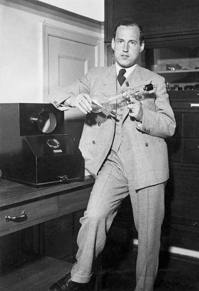
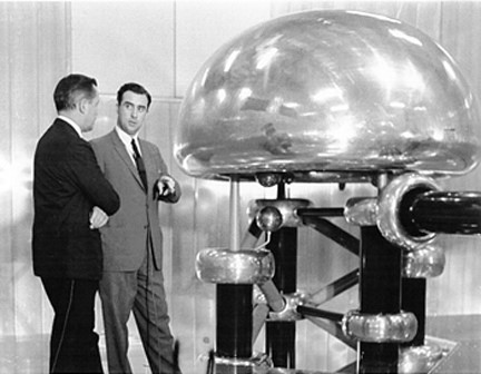
\(\newcommand{\avec}{\mathbf a}\) \(\newcommand{\bvec}{\mathbf b}\) \(\newcommand{\cvec}{\mathbf c}\) \(\newcommand{\dvec}{\mathbf d}\) \(\newcommand{\dtil}{\widetilde{\mathbf d}}\) \(\newcommand{\evec}{\mathbf e}\) \(\newcommand{\fvec}{\mathbf f}\) \(\newcommand{\nvec}{\mathbf n}\) \(\newcommand{\pvec}{\mathbf p}\) \(\newcommand{\qvec}{\mathbf q}\) \(\newcommand{\svec}{\mathbf s}\) \(\newcommand{\tvec}{\mathbf t}\) \(\newcommand{\uvec}{\mathbf u}\) \(\newcommand{\vvec}{\mathbf v}\) \(\newcommand{\wvec}{\mathbf w}\) \(\newcommand{\xvec}{\mathbf x}\) \(\newcommand{\yvec}{\mathbf y}\) \(\newcommand{\zvec}{\mathbf z}\) \(\newcommand{\rvec}{\mathbf r}\) \(\newcommand{\mvec}{\mathbf m}\) \(\newcommand{\zerovec}{\mathbf 0}\) \(\newcommand{\onevec}{\mathbf 1}\) \(\newcommand{\real}{\mathbb R}\) \(\newcommand{\twovec}[2]{\left[\begin{array}{r}#1 \\ #2 \end{array}\right]}\) \(\newcommand{\ctwovec}[2]{\left[\begin{array}{c}#1 \\ #2 \end{array}\right]}\) \(\newcommand{\threevec}[3]{\left[\begin{array}{r}#1 \\ #2 \\ #3 \end{array}\right]}\) \(\newcommand{\cthreevec}[3]{\left[\begin{array}{c}#1 \\ #2 \\ #3 \end{array}\right]}\) \(\newcommand{\fourvec}[4]{\left[\begin{array}{r}#1 \\ #2 \\ #3 \\ #4 \end{array}\right]}\) \(\newcommand{\cfourvec}[4]{\left[\begin{array}{c}#1 \\ #2 \\ #3 \\ #4 \end{array}\right]}\) \(\newcommand{\fivevec}[5]{\left[\begin{array}{r}#1 \\ #2 \\ #3 \\ #4 \\ #5 \\ \end{array}\right]}\) \(\newcommand{\cfivevec}[5]{\left[\begin{array}{c}#1 \\ #2 \\ #3 \\ #4 \\ #5 \\ \end{array}\right]}\) \(\newcommand{\mattwo}[4]{\left[\begin{array}{rr}#1 \amp #2 \\ #3 \amp #4 \\ \end{array}\right]}\) \(\newcommand{\laspan}[1]{\text{Span}\{#1\}}\) \(\newcommand{\bcal}{\cal B}\) \(\newcommand{\ccal}{\cal C}\) \(\newcommand{\scal}{\cal S}\) \(\newcommand{\wcal}{\cal W}\) \(\newcommand{\ecal}{\cal E}\) \(\newcommand{\coords}[2]{\left\{#1\right\}_{#2}}\) \(\newcommand{\gray}[1]{\color{gray}{#1}}\) \(\newcommand{\lgray}[1]{\color{lightgray}{#1}}\) \(\newcommand{\rank}{\operatorname{rank}}\) \(\newcommand{\row}{\text{Row}}\) \(\newcommand{\col}{\text{Col}}\) \(\renewcommand{\row}{\text{Row}}\) \(\newcommand{\nul}{\text{Nul}}\) \(\newcommand{\var}{\text{Var}}\) \(\newcommand{\corr}{\text{corr}}\) \(\newcommand{\len}[1]{\left|#1\right|}\) \(\newcommand{\bbar}{\overline{\bvec}}\) \(\newcommand{\bhat}{\widehat{\bvec}}\) \(\newcommand{\bperp}{\bvec^\perp}\) \(\newcommand{\xhat}{\widehat{\xvec}}\) \(\newcommand{\vhat}{\widehat{\vvec}}\) \(\newcommand{\uhat}{\widehat{\uvec}}\) \(\newcommand{\what}{\widehat{\wvec}}\) \(\newcommand{\Sighat}{\widehat{\Sigma}}\) \(\newcommand{\lt}{<}\) \(\newcommand{\gt}{>}\) \(\newcommand{\amp}{&}\) \(\definecolor{fillinmathshade}{gray}{0.9}\)Scanning tunneling microscopy (STM) is a powerful instrument that allows one to image the sample surface at the atomic level. As the first generation of scanning probe microscopy (SPM), STM paves the way for the study of nano-science and nano-materials. For the first time, researchers could obtain atom-resolution images of electrically conductive surfaces as well as their local electric structures. Because of this milestone invention, Gerd Binnig (Figure \(\PageIndex{1}\)) and Heinrich Rohrer (Figure \(\PageIndex{2}\)) won the Nobel Prize in Physics in 1986.


Principles of Scanning Tunneling Microscopy
The key physical principle behind STM is the tunneling effect. In terms of their wave nature, the electrons in the surface atoms actually are not as tightly bonded to the nucleons as the electrons in the atoms of the bulk. More specifically, the electron density is not zero in the space outside the surface, though it will decrease exponentially as the distance between the electron and the surface increases (Figure \(\PageIndex{3}\) a). So, when a metal tip approaches to a conductive surface within a very short distance, normally just a few Å, their perspective electron clouds will starting to overlap, and generate tunneling current if a small voltage is applied between them, as shown in Figure \(\PageIndex{3}) b.

When we consider the separation between the tip and the surface as an ideal one-dimensional tunneling barrier, the tunneling probability, or the tunneling current I, will depend largely on s, the distance between the tip and surface, \ref{1}, where m is the electron mass, e the electron charge, h the Plank constant, ϕ the averaged work function of the tip and the sample, and V the bias voltage.
\[ I \propto e^{-2s\ [2m/h^{2} (<\phi >\ -\ e|V|/2)]^{1/2}} \label{1} \]
A simple calculation will show us how strongly the tunneling current is affected by the distance (s). If s is increased by ∆s = 1 Å, \ref{2} and \ref{3}.
\[ \Delta I\ =\ e^{-2k_{0} \Delta s} \label{2} \]
\[ k_{0}\ =\ [2m/h^{2} (<\phi >\ -\ e|V|/2)]^{1/2} \label{3} \]
Usually (<ϕ> -e|V|/2) is about 5 eV, which k0 about 1 Å-1, then ∆I/I = 1/8. That means, if s changes by 1 Å, the current will change by one order of the magnitude. That’s the reason why we can get atom-level image by measuring the tunneling current between the tip and the sample.
In a typical STM operation process, the tip is scanning across the surface of sample in x-y plain, the instrument records the x-y position of the tip, measures the tunneling current, and control the height of the tip via a feedback circuit. The movements of the tip in x, y and z directions are all controlled by piezo ceramics, which can be elongated or shortened according to the voltage applied on them.
Normally, there are two modes of operation for STM, constant height mode and constant current mode. In constant height mode, the tip stays at a constant height when it scans through the sample, and the tunneling current is measured at different (x, y) position (Figure \(\PageIndex{4}\)b). This mode can be applied when the surface of sample is very smooth. But, if the sample is rough, or has some large particles on the surface, the tip may contact with the sample and damage the surface. In this case, the constant current mode is applied. During this scanning process, the tunneling current, namely the distance between the tip and the sample, is settled to an unchanged target value. If the tunneling current is higher than that target value, that means the height of the sample surface is increasing, the distance between the tip and sample is decreasing. In this situation, the feedback control system will respond quickly and retract the tip. Conversely, if the tunneling current drops below the target value, the feedback control will have the tip closer to the surface. According to the output signal from feedback control, the surface of the sample can be imaged.
Comparison of Atomic Force Microscopy (AFM) and Scanning Tunneling Microscopy (STM)
Both AFM and STM are widely used in nano-science. According to the different working principles though, they have their own advantages and disadvantages when measuring specific properties of sample (Table \(\PageIndex{1}\)). STM requires an electric circuit including the tip and sample to let the tunneling current go through. That means, the sample for STM must be conducting. In case of AFM however, it just measures the deflection of the cantilever caused by the van der Waals forces between the tip and sample. Thus, in general any kind of sample can be used for AFM. But, because of the exponential relation of the tunneling current and distance, STM has a better resolution than AFM. In STM image one can actually “see” an individual atom, while in AFM it’s almost impossible, and the quality of AFM image is largely depended on the shape and contact force of the tip. In some cases, the measured signal would be rather complicated to interpret into morphology or other properties of sample. On the other side, STM can give straight forward electric property of the sample surface.
| AFM | STM | |
| Sample Requirement | - | Conducting |
| Work environment | Air, liquid | Vacuum |
| Lateral resolution | ~1 nm | ~0.1 nm |
| Vertical resolution | ~0.05 nm | ~0.05 nm |
| Working mode | Tapping, contact | Constant current, constant height |
Applications of Scanning Tunneling Microscopy in Nanoscience
STM provides a powerful method to detect the surface of conducting and semi-conducting materials. Recently STM can also be applied in the imaging of insulators, superlattice assemblies and even the manipulation of molecules on surface. More importantly, STM can provide the surface structure and electric property of surface at atomic resolution, a true breakthrough in the development of nano-science. In this sense, the data collected from STM could reflect the local properties even of single molecule and atom. With these valuable measurement data, one could give a deeper understanding of structure-property relations in nanomaterials.
An excellent example is the STM imaging of graphene on Ru(0001), as shown in Figure \(\PageIndex{4}\). Clearly seen is the superstructure with a periodicity of ~30 Å , coming from the lattice mismatch of 12 unit cells of the graphene and 11 unit cells of the underneath Ru(0001) substrate. This so-called moiré structure can also be seen in other systems when the adsorbed layers have strong chemical bonds within the layer and weak interaction with the underlying surface. In this case, the periodic superstructure seen in graphene tells us that the formed graphene is well crystallized and expected to have high quality.
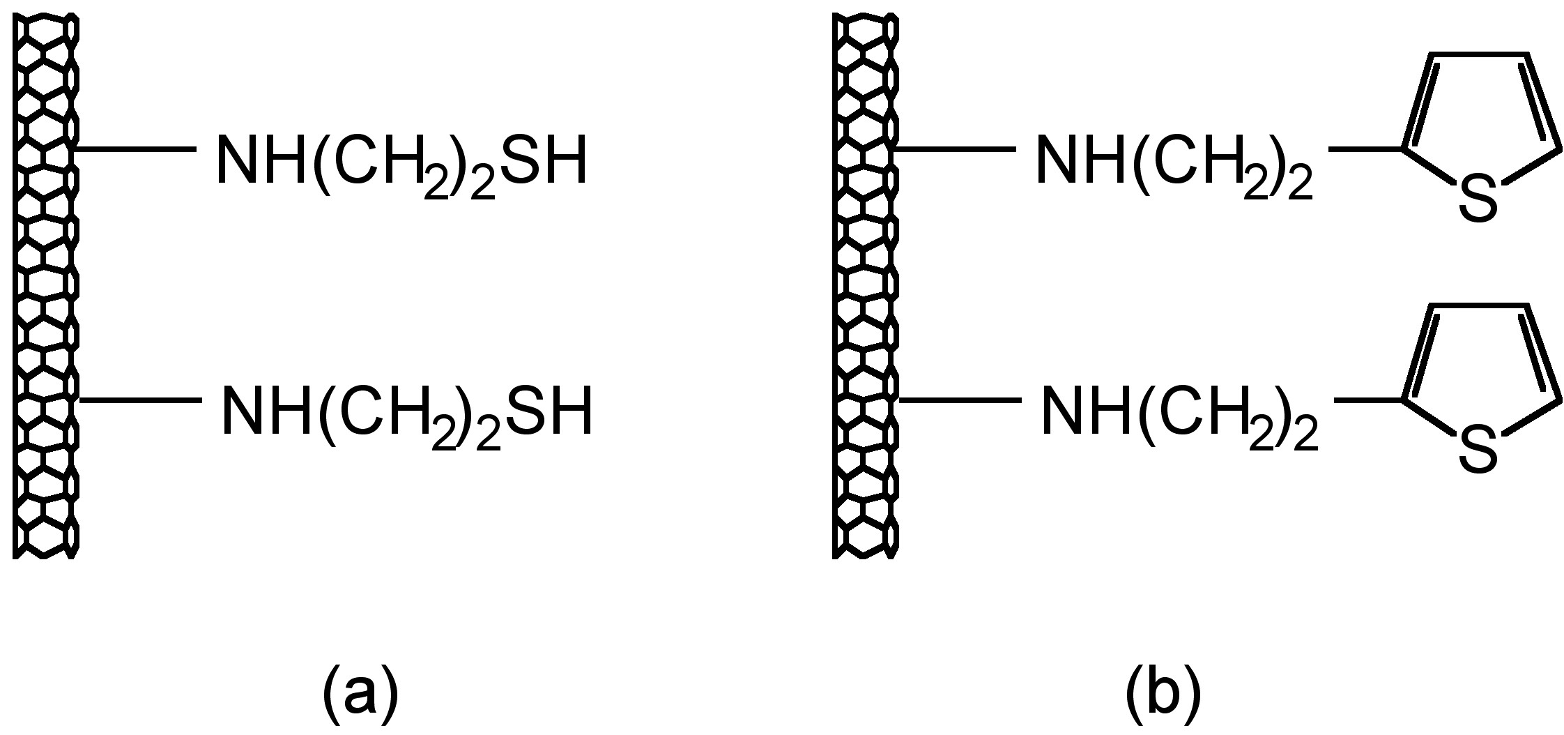
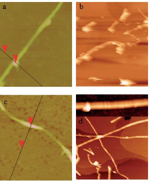
Another good example is shown to see that the measurement from STM could tell us the bonding information in single-molecular level. In thiol- and thiophene-functionalization of single-wall carbon nanotubes (SWNTs), the use of Au nanoparticles as chemical markers for AFM gives misleading results, while STM imaging could give correct information of substituent location. From AFM image, Au-thiol-SWNT (Figure \(\PageIndex{6}\)a) shows that most of the sidewalls are unfunctionalized, while Au-thiophene-SWNT (Figure \(\PageIndex{6}\) c)shows long bands of continuous functionalized regions on SWNT. This could lead to the estimation that thiophene is better functionalized to SWNT than thiol. Yet, if we look up to the STM image (Figure \(\PageIndex{6}\)b and d), in thiol-SWNTs the multiple functional groups are tightly bonded in about 5 - 25 nm, while in thiophene-SWNTs the functionalization is spread out uniformly along the whole length of SWNT. This information indicates that actually the functionalization levels of thiol- and thiophene-SWNTs are comparable. The difference is that, in thiol-SWNTs, functional groups are grouped together and each group is bonded to a single gold nanoparticle, while in thiophene-SWNTs, every individual functional group is bonded to a nanoparticle.
Adaptations to Scanning Tunneling Microscopy
Scanning tunneling microscopy (STM) is a relatively recent imaging technology that has proven very useful for determining the topography of conducting and semiconducting samples with angstrom (Å) level precision. STM was invented by Gerd Binnig (Figure \(\PageIndex{7}\)) and Heinrich Rohrer (Figure \(\PageIndex{8}\)), who both won the 1986 Nobel Prize in physics for their technological advances.

The main component of a scanning tunneling microscope is a rigid metallic probe tip, typically composed of tungsten, connected to a piezodrive containing three perpendicular piezoelectric transducers (Figure \(\PageIndex{9}\)). The tip is brought within a fraction of a nanometer of an electrically conducting sample. At close distances, the electron clouds of the metal tip overlap with the electron clouds of the surface atoms (Figure \(\PageIndex{9}\) inset). If a small voltage is applied between the tip and the sample a tunneling current is generated. The magnitude of this tunneling current is dependent on the bias voltage applied and the distance between the tip and the surface. A current amplifier can covert the generated tunneling current into a voltage. The magnitude of the resulting voltage as compared to the initial voltage can then be used to control the piezodrive, which controls the distance between the tip and the surface (i.e., the z direction). By scanning the tip in the x and y directions, the tunneling current can be measured across the entire sample. The STM system can operate in either of two modes: Constant height or constant current
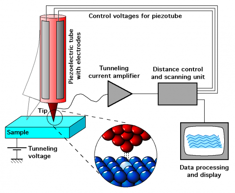
In constant height mode, the tip is fixed in the z direction and the change in tunneling current as the tip changes in the x,y direction is collected and plotted to describe the change in topography of the sample. This method is dangerous for use in samples with fluctuations in height as the fixed tip might contact and destroy raised areas of the sample. A common method for non-uniformly smooth samples is constant current mode. In this mode, a target current value, called the set point, is selected and the tunneling current data gathered from the sample is compared to the target value. If the collected voltage deviates from the set point, the tip is moved in the z direction and the voltage is measured again until the target voltage is reached. The change in the z direction required to reach the set point is recorded across the entire sample and plotted as a representation of the topography of the sample. The height data is typically displayed as a gray scale image of the topography of the sample, where lighter areas typically indicate raised sample areas and darker spots indicate protrusions. These images are typically colored for better contrast.
The standard method of STM, described above, is useful for many substances (including high precision optical components, disk drive surfaces, and buckyballs) and is typically used under ultrahigh vacuum to avoid contamination of the samples from the surrounding systems. Other sample types, such as semiconductor interfaces or biological samples, need some enhancements to the traditional STM apparatus to yield more detailed sample information. Three such modifications, spin-polarized STM (SP-STM), ballistic electron emission microscopy (BEEM) and photon STM (PSTM) are summarized in Table \(\PageIndex{2}\) and in described in detail below.
| Name | Alterations to Conventional STM | Sample Types | Limitations |
| STM | None | Conducting surface | Rigidity of probe |
| SP-STM | Magnetized STM tip | Magnetic | Needs to be overlaid with STM, magnetized tip type |
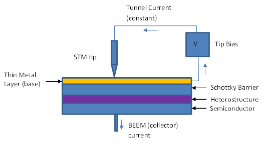
| BEEM | Three-terminal with base electrode and current collector | Interfaces | Voltage, changes due to barrier height |
| PSTM | Optical fiber tip | Biological | Optical tip and psrim manufacture |
Spin Polarized STM
Spin-polarized scanning tunneling microscopy (SP-STM) can be used to provide detailed information of magnetic phenomena on the single-atom scale. This imaging technique is particularly important for accurate measurement of superconductivity and high-density magnetic data storage devices. In addition, SP-STM, while sensitive to the partial magnetic moments of the sample, is not a field-sensitive technique and so can be applied in a variety of different magnetic fields.
Device setup and sample preparation
In SP-STM, the STM tip is coated with a thin layer of magnetic material. As with STM, voltage is then applied between tip and sample resulting in tunneling current. Atoms with partial magnetic moments that are aligned in the same direction as the partial magnetic moment of the atom at the very tip of the STM tip show a higher magnitude of tunneling current due to the interactions between the magnetic moments. Likewise, atoms with partial magnetic moments opposite that of the atom at the tip of the STM tip demonstrate a reduced tunneling current (Figure \(\PageIndex{10}\)). A computer program can then translate the change in tunneling current to a topographical map, showing the spin density on the surface of the sample.
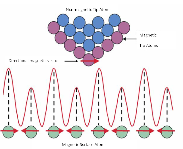
The sensitivity to magnetic moments depends greatly upon the direction of the magnetic moment of the tip, which can be controlled by the magnetic properties of the material used to coat the outermost layer of the tungsten STM probe. A wide variety of magnetic materials have been studied as possible coatings, including both ferromagnetic materials, such as a thin coat of iron or of gadolinium, and antiferromagnetic materials such as chromium. Another method that has been used to make a magnetically sensitive probe tip is irradiation of a semiconducting GaAs tip with high energy circularly polarized light. This irradiation causes a splitting of electrons in the GaAs valence band and population of the conduction band with spin-polarized electrons. These spin-polarized electrons then provide partial magnetic moments which in turn influence the tunneling current generated by the sample surface.
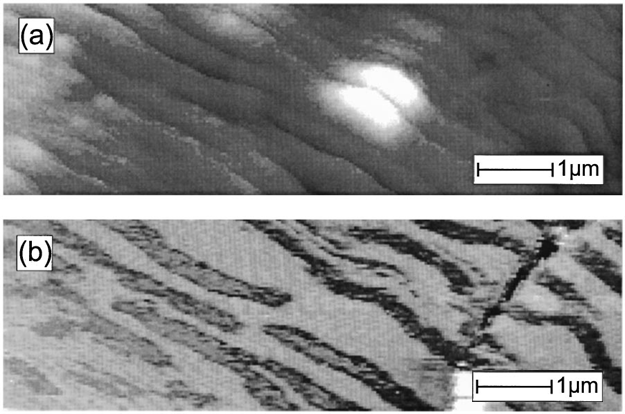
Sample preparation for SP-STM is essentially the same as for STM. SP-STM has been used to image samples such as thin films and nanoparticle constructs as well as determining the magnetic topography of thin metallic sheets such as in Figure \(\PageIndex{11}\). The upper image is a traditional STM image of a thin layer of cobalt, which shows the topography of the sample. The second image is an SP-STM image of the same layer of cobalt, which shows the magnetic domain of the sample. The two images, when combined provide useful information about the exact location of the partial magnetic moments within the sample.
Limitations
One of the major limitations with SP-STM is that both distance and partial magnetic moment yield the same contrast in a SP-STM image. This can be corrected by combination with conventional STM to get multi-domain structures and/or topological information which can then be overlaid on top of the SP-STM image, correcting for differences in sample height as opposed to magnetization.
The properties of the magnetic tip dictate much of the properties of the technique itself. If the outermost atom of the tip is not properly magnetized, the technique will yield no more information than a traditional STM. The direction of the magnetization vector of the tip is also of great importance. If the magnetization vector of the tip is perpendicular to the magnetization vector of the sample, there will be no spin contrast. It is therefore important to carefully choose the coating applied to the tungsten STM tip in order to align appropriately with the expected magnetic moments of the sample. Also, the coating makes the magnetic tips more expensive to produce than standard STM tips. In addition, these tips are often made of mechanically soft materials, causing them to wear quickly and require a high cost of maintenance.
Ballistic Electron Emission Microscopy
Ballistic electron emission microscopy (BEEM) is a technique commonly used to image semiconductor interfaces. Conventional surface probe techniques can provide detailed information on the formation of interfaces, but lack the ability to study fully formed interfaces due to inaccessibility to the surface. BEEM allows for the ability to obtain a quantitative measure of electron transport across fully formed interfaces, something necessary for many industrial applications.
Device Setup and Sample Preparation
BEEM utilizes STM with a three-electrode configuration, as seen in Figure \(\PageIndex{12}\). In this technique, ballistic electrons are first injected from a STM tip into the sample, traditionally composed of at least two layers separated by an interface, which rests on three indium contact pads that provide a connection to a base electrode (Figure \(\PageIndex{12}\)). As the voltage is applied to the sample, electrons tunnel across the vacuum and through the first layer of the sample, reaching the interface, and then scatter. Depending on the magnitude of the voltage, some percentage of the electrons tunnel through the interface, and can be collected and measured as a current at a collector attached to the other side of the sample. The voltage from the STM tip is then varied, allowing for measurement of the barrier height. The barrier height is defined as the threshold at which electrons will cross the interface and are measurable as a current in the far collector. At a metal/n-type semiconductor interface this is the difference between the conduction band minimum and the Fermi level. At a metal/p-type semiconductor interface this is the difference between the valence band maximum of the semiconductor and the metal Fermi level. If the voltage is less than the barrier height, no electrons will cross the interface and the collector will read zero. If the voltage is greater than the barrier height, useful information can be gathered about the magnitude of the current at the collector as opposed to the initial voltage.
Samples are prepared from semiconductor wafers by chemical oxide growth-strip cycles, ending with the growth of a protective oxide layer. Immediately prior to imaging the sample is spin-etched in an inert environment to remove oxides of oxides and then transferred directly to the ultra-high vacuum without air exposure. The BEEM apparatus itself is operated in a glove box under inert atmosphere and shielded from light.
Nearly any type of semiconductor interface can be imaged with BEEM. This includes both simple binary interfaces such as Au/n-Si(100) and more chemically complex interfaces such as Au/n-GaAs(100), such as seen in Figure \(\PageIndex{13}\).
Limitations
Expected barrier height matters a great deal in the desired setup of the BEEM apparatus. If it is necessary to measure small collector currents, such as with an interface of high-barrier-height, a high-gain, low-noise current preamplifier can be added to the system. If the interface is of low-barrier-height, the BEEM apparatus can be operated at very low temperatures, accomplished by immersion of the STM tip in liquid nitrogen and enclosure of the BEEM apparatus in a nitrogen-purged glove box.
Photon STM
Photon scanning tunneling microscopy (PSTM) measures light to determine more information about characteristic sample topography. It has primarily been used as a technique to measure the electromagnetic interaction of two metallic objects in close proximity to one another and biological samples, which are both difficult to measure using many other common surface analysis techniques.
Device Setup and Sample Preparation
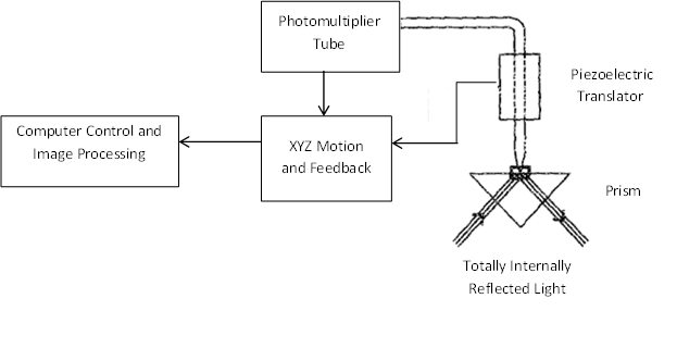
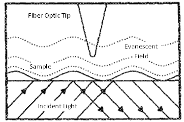
This technique works by measuring the tunneling of photons to an optical tip. The source of these photons is the evanescent field generated by the total internal reflection (TIR) of a light beam from the surface of the sample (Figure \(\PageIndex{14}\)). This field is characteristic of the sample material on the TIR surface, and can be measured by a sharpened optical fiber probe tip where the light intensity is converted to an electrical signal (Figure \(\PageIndex{15}\)). Much like conventional STM, the force of this electrical signal modifies the location of the tip in relation to the sample. By mapping these modifications across the entire sample, the topography can be determined to a very accurate degree as well as allowing for calculations of polarization, emission direction and emission time.
In PSTM, the vertical resolution is governed only by the noise, as opposed to conventional STM where the vertical resolution is limited by the tip dimensions. Therefore, this technique provides advantages over more conventional STM apparatus for samples where subwavelength resolution in the vertical dimension is a critical measurement, including fractal metal colloid clusters, nanostructured materials and simple organic molecules.
Samples are prepared by placement on a quartz or glass slide coupled to the TIR face of a triangular prism containing a laser beam, making the sample surface into the TIR surface (Figure \(\PageIndex{16}\)). The optical fiber probe tips are constructed from UV grade quartz optical fibers by etching in HF acid to have nominal end diameters of 200 nm or less and resemble either a truncated cone or a paraboloid of revolution (Figure \(\PageIndex{16}\)).
PSTM shows much promise in the imaging of biological materials due to the increase in vertical resolution and the ability to measure a sample within a liquid environment with a high index TIR substrate and probe tip. This would provide much more detailed information about small organisms than is currently available.
Limitations
The majority of the limitations in this technique come from the materials and construction of the optical fibers and the prism used in the sample collection. The sample needs to be kept at low temperatures, typically around 100K, for the duration of the imaging and therefore cannot decompose or be otherwise negatively impacted by drastic temperature changes.
Conclusion
Scanning tunneling microscopy can provide a great deal of information into the topography of a sample when used without adaptations, but with adaptations, the information gained is nearly limitless. Depending on the likely properties of your sample surface, SP-STM, BEEM and PSTM can provide much more accurate topographical pictures than conventional forms of STM (Table \(\PageIndex{2}\)). All of these adaptations to STM have their limitations and all work within relatively specialized categories and subsets of substances, but they are very strong tools that are constantly improving to provide more useful information about materials to the nanometer scale.
Scanning Transmission Electron Microscope- Electron Energy Loss Spectroscopy (STEM-EELS)
History
STEM-EELS is a terminology abbreviation for scanning transmission electron microscopy (STEM) coupled with electron energy loss spectroscopy (EELS). It works by combining two instruments, obtaining an image through STEM and applying EELS to detect signals on the specific selected area of the image. Therefore, it can be applied for many research, such as characterizing morphology, detecting different elements, and different valence state. The first STEM was built by Baron Manfred von Arden (Figure \(\PageIndex{17}\)) in around 1983, since it was just the prototype of STEM, it was not as good as transmission electron microscopy (TEM) by that time. Development of STEM was stagnant until the field emission gun was invented by Albert Crewe (Figure \(\PageIndex{18}\)) in 1970s; he also came with the idea of annular dark field detector to detect atoms. In 1997, its resolution increased to 1.9 Å, and further increased to 1.36 Å in 2000. 4D STEM-EELS was developed recently, and this type of 4D STEM-EELS has high brightness STEM equipped with a high acquisition rate EELS detector, and a rotation holder. The rotation holder plays quite an important role to achieve this 4D aim, because it makes observation of the sample in 360° possible, the sample could be rotated to acquire the sample’s thickness. High acquisition rate EELS enables this instrument the acquisition of the pixel spectrum in a few minutes.
Basics of STEM-EELS
Interaction between Electrons and Sample
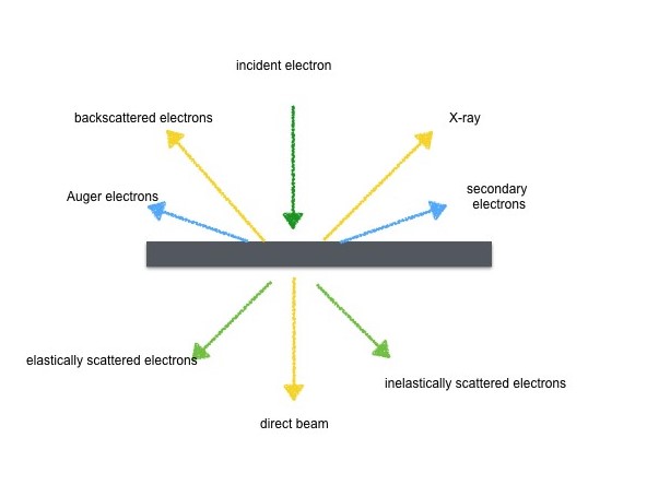
When electrons interact with the samples, the interaction between those two can be classified into two types, namely, elastic and inelastic interactions (Figure \(\PageIndex{19}\)). In the elastic interaction, if electrons do not interact with the sample and pass through it, these electrons will contribute to the direct beam. The direct beam can be applied in STEM. In another case, electrons’ moving direction in the sample is guided by the Coulombic force; the strength of the force is decided by charge and the distance between electrons and the core. In both cases, these is no energy transfer from electrons to the samples, that’s the reason why it is called elastic interaction. In inelastic interaction, energy transfers from incident electrons to the samples, thereby, losing energy. The lost energy can be measured and how many electrons amounted to this energy can also be measured, and these data yield the electron energy loss spectrum (EELS).
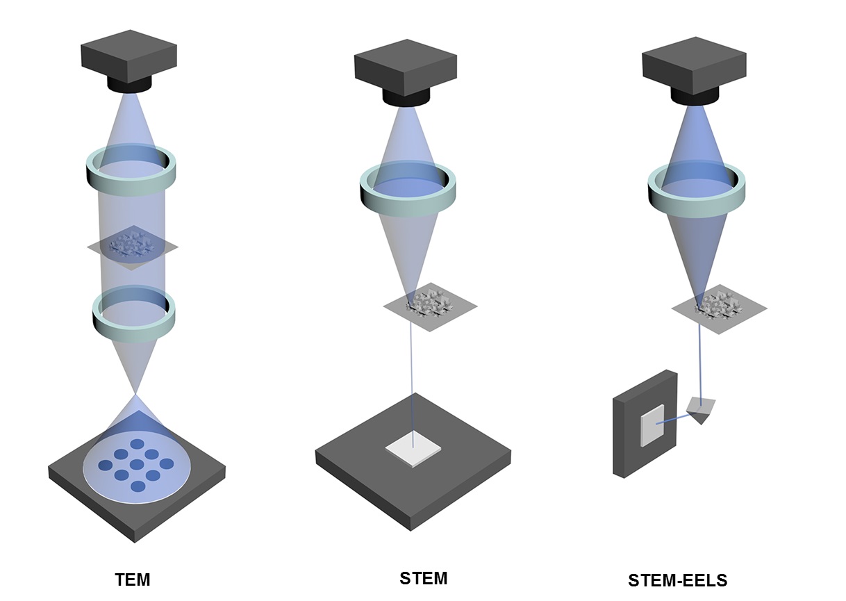
How do TEM, STEM and STEM-EELS work?
In transmission electron microscopy (TEM), a beam of electrons is emitted from tungsten source and then accelerated by electromagnetic field. Then with the aid of lens condenser, the beam will focus on and pass through the sample. Finally, the electrons will be detected by a charge-coupled device (CCD) and produce images, Figure \(\PageIndex{20}\). STEM works differently from TEM, the electron beam focuses on a specific spot of the sample and then raster scans the sample pixel by pixel, the detector will collect the transmitted electrons and visualize the sample. Moreover, STEM-EELS allows to analyze these electrons, the transmitted electrons could be characterized by adding a magnetic prism, the more energy the electrons lose, the more they will be deflected. Therefore, STEM-EELS can be used to characterize the chemical properties of thin samples.
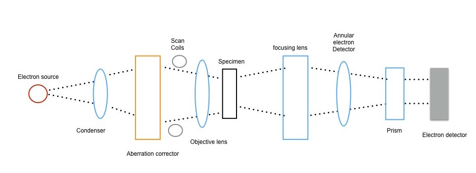
Principles of STEM-EELS
A brief illustration of STEM-EELS is displayed in Figure \(\PageIndex{21}\). The electron source provides electrons, and it usually comes from a tungsten source located in a strong electrical field. The electron field will provide electrons with high energy. The condenser and the object lens also promote electrons forming into a fine probe and then raster scanning the specimen. The diameter of the probe will influence STEM’s spatial resolution, which is caused by the lens aberrations. Lens aberration results from the refraction difference between light rays striking the edge and center point of the lens, and it also can happen when the light rays pass through with different energy. Base on this, an aberration corrector is applied to increase the objective aperture, and the incident probe will converge and increase the resolution, then promote sensitivity to single atoms. For the annular electron detector, the installment sequence of detectors is a bright field detector, a dark field detector and a high angle annular dark field detector. Bright field detector detects the direct beam that transmits through the specimen. Annular dark field detector collects the scattered electrons, which only go through at an aperture. The advantage of this is that it will not influence the EELS to detect signals from direct beam. High angle annular dark field detector collects electrons which are Rutherford scattering (elastic scattering of charged electrons), and its signal intensity is related with the square of atomic number (Z). So, it is also named as Z-contrast image. The unique point about STEM in acquiring image is that the pixels in image are obtained in a point by point mode by scanning the probe. EELS analysis is based on the energy loss of the transmitted electrons, so the thickness of the specimen will influence the detecting signal. In other words, if the specimen is too thick, the intensity of plasmon signal will decrease and may cause difficulty distinguishing these signals from the background.
Typical features of EELS Spectra
As shown in Figure \(\PageIndex{22}\), a significant peak appears at energy zero in EELS spectra and is therefore called zero-loss peak. Zero-loss peak represents the electrons which undergo elastic scattering during the interaction with specimen. Zero-loss peak can be used to determine the thickness of specimen according to \ref{4}, where t stands for the thickness, λinel is inelastic mean free path, It stands for the total intensity of the spectrum and IZLP is the intensity of zero loss peak.
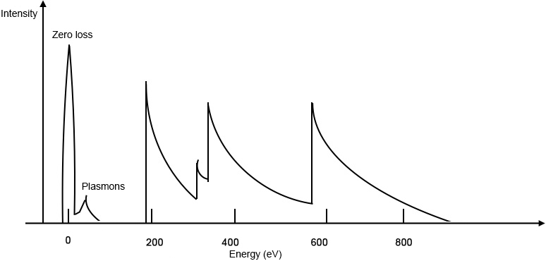
\[ t\ =\ \lambda _{inel}\ ln[I_{t}/I_{ZLP}] \label{4} \]
The low loss region is also called valence EELS. In this region,valence electrons will be excited to the conduction band. Valence EELS can provide the information about band structure, bandgap, and optical properties. In the low loss region, plasmon peak is the most important. Plasmon is a phenomenon originates from the collective oscillation of weakly bound electrons. Thickness of the sample will influence the plasmon peak. The incident electrons will go through inelastic scattering several times when they interact with a very thick sample, and then result in convoluted plasmon peaks. It is also the reason why STEM-EELS favors sample with low thickness (usually less than 100 nm).
The high loss region is characterized by the rapidly increasing intensity with a gradually falling, which called ionization edge. The onset of ionization edges equals to the energy that inner shell electron needs to be excited from the ground state to the lowest unoccupied state. The amount of energy is unique for different shells and elements. Thus, this information will help to understand the bonding, valence state, composition and coordination information.
Energy resolution affects the signal to background ratio in the low loss region and is used to evaluate EELS spectrum. Energy resolution is based on the full width at half maximum of zero-loss peak.
Background signal in the core-loss region is caused by plasmon peaks and core-loss edges, and can be described by the following power law, \ref{5}, where IBG stands for the background signal, E is the energy loss, A is the scaling constant and r is the slope exponent:
\[ I_{BG}\ =\ AE^{-r} \label{5} \]
Therefore, when quantification the spectra data, the background signal can be removed by fitting pre-edge region with the above-mentioned equation and extrapolating it to the post-edge region.
Advantages and Disadvantages of STEM-EELS
STEM-EELS has advantages over other instruments, such as the acquisition of high resolution of images. For example, the operation of TEM on samples sometimes result in blurring image and low contrast because of chromatic aberration. STEM-EELS equipped with aberration corrector, will help to reduce the chromatic aberration and obtain high quality image even at atomic resolution. It is very direct and convenient to understand the electron distributions on surface and bonding information. STEM-EELS also has the advantages in controlling the spread of energy. So, it becomes much easier to study the ionization edge of different material.
Even though STEM-EELS does bring a lot of convenience for research in atomic level, it still has limitations to overcome. One of the main limitation of STEM-EELS is controlling the thickness of the sample. As discussed above, EELS detects the energy loss of electrons when they interact with samples and the specimen, then the thickness of samples will impact on the energy lost detection. Simplify, if the sample is too thick, then most of the electrons will interact with the sample, signal to background ratio and edge visibility will decrease. Thus, it will be hard to tell the chemical state of the element. Another limitation is due to EELS needs to characterize low-loss energy electrons, which high vacuum condition is essential for characterization. To achieve such a high vacuum environment, high voltage is necessary. STEM-EELS also requires the sample substrates to be conductive and flat.
Application of STEM-EELS
STEM-EELS can be used to detect the size and distribution of nanoparticles on a surface. For example, CoO on MgO catalyst nanoparticles may be prepared by hydrothermal methods. The size and distribution of nanoparticles will greatly influence the catalytic properties, and the distribution and morphology change of CoO nanoparticles on MgO is important to understand. Co L3/L2 ratios display uniformly around 2.9, suggesting that Co2+ dominates the electron state of Co. The results show that the ratios of O:(Co+Mg) and Mg:(Co+Mg) are not consistence, indicating that these three elements are in a random distribution. STEM-EELS mapping images results further confirm the non-uniformity of the elemental distribution, consistent with a random distribution of CoO on the MgO surface (Figure \(\PageIndex{23}\)).
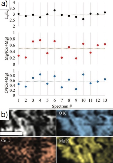
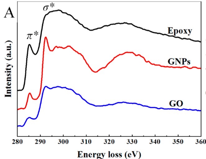
Figure \(\PageIndex{24}\) shows the K-edge absorption of carbon and transition state information could be concluded. Typical carbon based materials have the features of the transition state, such that 1s transits to π* state and 1s to σ* states locate at 285 and 292 eV, respectively. The two-transition state correspond to the electrons in the valence band electrons being excited to conduction state. Epoxy exhibits a sharp peak around 285.3 eV compared to GO and GNPs. Meanwhile, GNPs have the sharpest peak around 292 eV, suggesting the most C atoms in GNPs are in 1s to σ* state. Even though GO is in oxidation state, part of its carbon still behaves 1s transits to π*.
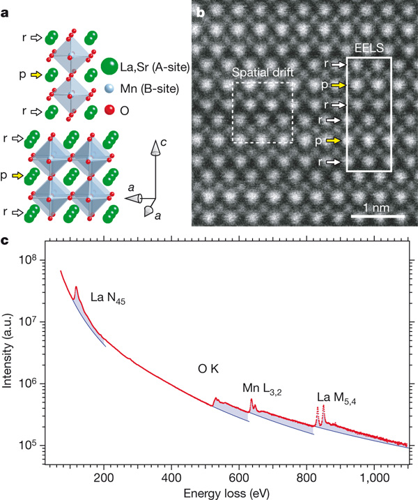
The annular dark filed (ADF) mode of STEM provides information about atomic number of the elements in a sample. For example, the ADF image of La1.2Sr1.8Mn2O7 (Figure \(\PageIndex{25}\) a and b) along [010] direction shows bright spots and dark spots, and even for bright spots (p and r), they display different levels of brightness. This phenomenon is caused by the difference in atomic numbers. Bright spots are La and Sr, respectively. Dark spots are Mn elements. O is too light to show on the image. EELS result shows the core-loss edge of La, Mn and O (Figure \(\PageIndex{25}\) c), but the researchers did not give information on core-loss edge of Sr, Sr has N2,3 edge at 29 eV and L3 edge at 1930 eV and L2 edge at 2010 eV.