8.2: Transmission Electron Microscopy
- Page ID
- 55918

\( \newcommand{\vecs}[1]{\overset { \scriptstyle \rightharpoonup} {\mathbf{#1}} } \)
\( \newcommand{\vecd}[1]{\overset{-\!-\!\rightharpoonup}{\vphantom{a}\smash {#1}}} \)
\( \newcommand{\id}{\mathrm{id}}\) \( \newcommand{\Span}{\mathrm{span}}\)
( \newcommand{\kernel}{\mathrm{null}\,}\) \( \newcommand{\range}{\mathrm{range}\,}\)
\( \newcommand{\RealPart}{\mathrm{Re}}\) \( \newcommand{\ImaginaryPart}{\mathrm{Im}}\)
\( \newcommand{\Argument}{\mathrm{Arg}}\) \( \newcommand{\norm}[1]{\| #1 \|}\)
\( \newcommand{\inner}[2]{\langle #1, #2 \rangle}\)
\( \newcommand{\Span}{\mathrm{span}}\)
\( \newcommand{\id}{\mathrm{id}}\)
\( \newcommand{\Span}{\mathrm{span}}\)
\( \newcommand{\kernel}{\mathrm{null}\,}\)
\( \newcommand{\range}{\mathrm{range}\,}\)
\( \newcommand{\RealPart}{\mathrm{Re}}\)
\( \newcommand{\ImaginaryPart}{\mathrm{Im}}\)
\( \newcommand{\Argument}{\mathrm{Arg}}\)
\( \newcommand{\norm}[1]{\| #1 \|}\)
\( \newcommand{\inner}[2]{\langle #1, #2 \rangle}\)
\( \newcommand{\Span}{\mathrm{span}}\) \( \newcommand{\AA}{\unicode[.8,0]{x212B}}\)
\( \newcommand{\vectorA}[1]{\vec{#1}} % arrow\)
\( \newcommand{\vectorAt}[1]{\vec{\text{#1}}} % arrow\)
\( \newcommand{\vectorB}[1]{\overset { \scriptstyle \rightharpoonup} {\mathbf{#1}} } \)
\( \newcommand{\vectorC}[1]{\textbf{#1}} \)
\( \newcommand{\vectorD}[1]{\overrightarrow{#1}} \)
\( \newcommand{\vectorDt}[1]{\overrightarrow{\text{#1}}} \)
\( \newcommand{\vectE}[1]{\overset{-\!-\!\rightharpoonup}{\vphantom{a}\smash{\mathbf {#1}}}} \)
\( \newcommand{\vecs}[1]{\overset { \scriptstyle \rightharpoonup} {\mathbf{#1}} } \)
\( \newcommand{\vecd}[1]{\overset{-\!-\!\rightharpoonup}{\vphantom{a}\smash {#1}}} \)
\(\newcommand{\avec}{\mathbf a}\) \(\newcommand{\bvec}{\mathbf b}\) \(\newcommand{\cvec}{\mathbf c}\) \(\newcommand{\dvec}{\mathbf d}\) \(\newcommand{\dtil}{\widetilde{\mathbf d}}\) \(\newcommand{\evec}{\mathbf e}\) \(\newcommand{\fvec}{\mathbf f}\) \(\newcommand{\nvec}{\mathbf n}\) \(\newcommand{\pvec}{\mathbf p}\) \(\newcommand{\qvec}{\mathbf q}\) \(\newcommand{\svec}{\mathbf s}\) \(\newcommand{\tvec}{\mathbf t}\) \(\newcommand{\uvec}{\mathbf u}\) \(\newcommand{\vvec}{\mathbf v}\) \(\newcommand{\wvec}{\mathbf w}\) \(\newcommand{\xvec}{\mathbf x}\) \(\newcommand{\yvec}{\mathbf y}\) \(\newcommand{\zvec}{\mathbf z}\) \(\newcommand{\rvec}{\mathbf r}\) \(\newcommand{\mvec}{\mathbf m}\) \(\newcommand{\zerovec}{\mathbf 0}\) \(\newcommand{\onevec}{\mathbf 1}\) \(\newcommand{\real}{\mathbb R}\) \(\newcommand{\twovec}[2]{\left[\begin{array}{r}#1 \\ #2 \end{array}\right]}\) \(\newcommand{\ctwovec}[2]{\left[\begin{array}{c}#1 \\ #2 \end{array}\right]}\) \(\newcommand{\threevec}[3]{\left[\begin{array}{r}#1 \\ #2 \\ #3 \end{array}\right]}\) \(\newcommand{\cthreevec}[3]{\left[\begin{array}{c}#1 \\ #2 \\ #3 \end{array}\right]}\) \(\newcommand{\fourvec}[4]{\left[\begin{array}{r}#1 \\ #2 \\ #3 \\ #4 \end{array}\right]}\) \(\newcommand{\cfourvec}[4]{\left[\begin{array}{c}#1 \\ #2 \\ #3 \\ #4 \end{array}\right]}\) \(\newcommand{\fivevec}[5]{\left[\begin{array}{r}#1 \\ #2 \\ #3 \\ #4 \\ #5 \\ \end{array}\right]}\) \(\newcommand{\cfivevec}[5]{\left[\begin{array}{c}#1 \\ #2 \\ #3 \\ #4 \\ #5 \\ \end{array}\right]}\) \(\newcommand{\mattwo}[4]{\left[\begin{array}{rr}#1 \amp #2 \\ #3 \amp #4 \\ \end{array}\right]}\) \(\newcommand{\laspan}[1]{\text{Span}\{#1\}}\) \(\newcommand{\bcal}{\cal B}\) \(\newcommand{\ccal}{\cal C}\) \(\newcommand{\scal}{\cal S}\) \(\newcommand{\wcal}{\cal W}\) \(\newcommand{\ecal}{\cal E}\) \(\newcommand{\coords}[2]{\left\{#1\right\}_{#2}}\) \(\newcommand{\gray}[1]{\color{gray}{#1}}\) \(\newcommand{\lgray}[1]{\color{lightgray}{#1}}\) \(\newcommand{\rank}{\operatorname{rank}}\) \(\newcommand{\row}{\text{Row}}\) \(\newcommand{\col}{\text{Col}}\) \(\renewcommand{\row}{\text{Row}}\) \(\newcommand{\nul}{\text{Nul}}\) \(\newcommand{\var}{\text{Var}}\) \(\newcommand{\corr}{\text{corr}}\) \(\newcommand{\len}[1]{\left|#1\right|}\) \(\newcommand{\bbar}{\overline{\bvec}}\) \(\newcommand{\bhat}{\widehat{\bvec}}\) \(\newcommand{\bperp}{\bvec^\perp}\) \(\newcommand{\xhat}{\widehat{\xvec}}\) \(\newcommand{\vhat}{\widehat{\vvec}}\) \(\newcommand{\uhat}{\widehat{\uvec}}\) \(\newcommand{\what}{\widehat{\wvec}}\) \(\newcommand{\Sighat}{\widehat{\Sigma}}\) \(\newcommand{\lt}{<}\) \(\newcommand{\gt}{>}\) \(\newcommand{\amp}{&}\) \(\definecolor{fillinmathshade}{gray}{0.9}\)TEM: An Overview
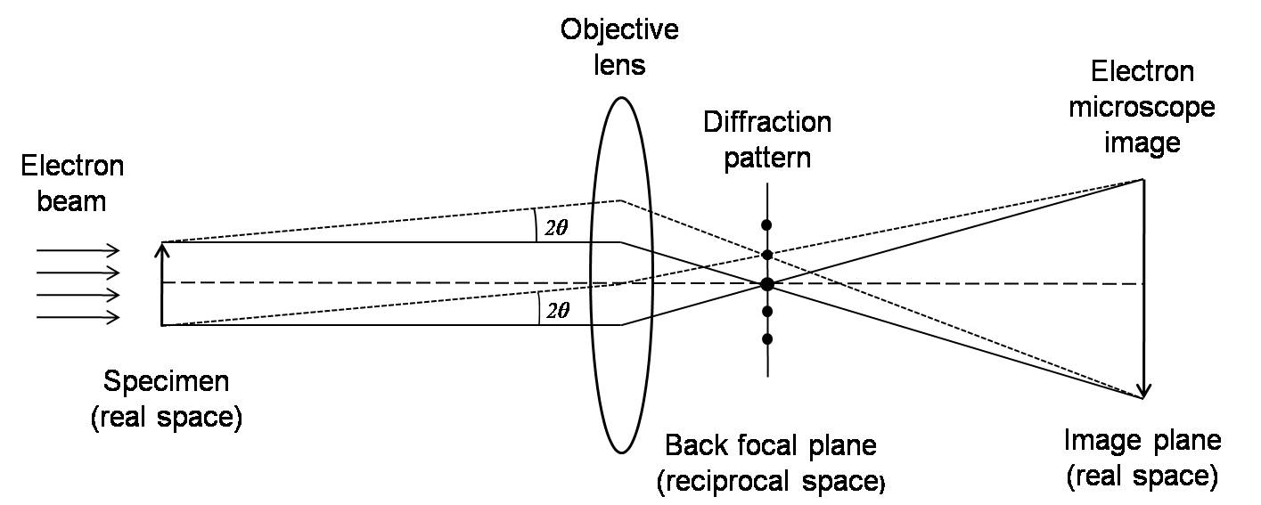
Transmission electron microscopy (TEM) is a form of microscopy which in which a beam of electrons transmits through an extremely thin specimen, and then interacts with the specimen when passing through it. The formation of images in a TEM can be explained by an optical electron beam diagram in Figure \(\PageIndex{1}\). TEMs provide images with significantly higher resolution than visible-light microscopes (VLMs) do because of the smaller de Broglie wavelength of electrons. These electrons allow for the examination of finer details, which are several thousand times higher than the highest resolution in a VLM. Nevertheless, the magnification provide in a TEM image is in contrast to the absorption of the electrons in the material, which is primarily due to the thickness or composition of the material.
When a crystal lattice spacing (d) is investigated with electrons with wavelength λ, diffracted waves will be formed at specific angles 2θ, satisfying the Bragg condition, \ref{1}.
\[ 2dsin\theta \ =\ \lambda \label{1} \]
The regular arrangement of the diffraction spots, the so-called diffraction pattern (DP), can be observed. While the transmitted and the diffracted beams interfere on the image plane, a magnified image (electron microscope image) appears. The plane where the DP forms is called the reciprocal space, which the image plane is called the real space. A Fourier transform can mathematically transform the real space to reciprocal space.
By adjusting the lenses (changing their focal lengths), both electron microscope images and DP can be observed. Thus, both observation modes can be successfully combined in the analysis of the microstructures of materials. For instance, during investigation of DPs, an electron microscope image is observed. Then, by inserting an aperture (selected area aperture), adjusting the lenses, and focusing on a specific area that we are interested in, we will get a DP of the area. This kind of observation mode is called a selected area diffraction. In order to investigate an electron microscope image, we first observe the DP. Then by passing the transmitted beam or one of the diffracted beams through a selected aperture and changing to the imaging mode, we can get the image with enhanced contrast, and precipitates and lattice defects can easily be identified.
Describing the resolution of a TEM in terms of the classic Rayleigh criterion for VLMs, which states that the smallest distance that can be investigated, δ, is given approximately by \ref{2}, where λ is the wavelength of the electrons, µ is the refractive index of the viewing medium, and β is the semi-angle of collection of the magnifying lens.
\[ \delta \ = \frac{0.61 \lambda }{\mu \ sin \beta} \label{2} \]
ccording to de Broglie’s ideas of the wave-particle duality, the particle momentum p is related to its wavelength λ through Planck’s constant h, \ref{3}.
\[ \lambda = \frac{h}{p} \label{3} \]
Momentum is given to the electron by accelerating it through a potential drop, V, giving it a kinetic energy, eV. This potential energy is equal to the kinetic energy of the electron, \ref{4}.
\[ eV\ =\ \frac{m_{o} u ^{2}}{2} \label{4} \]
Based upon the foregoing, we can equate the momentum (p) to the electron mass (mo), multiplied by the velocity (v) and substituting for v from \ref{5} i.e., \ref{6}.
\[ p\ =\ m_{o} u \ =\ (2m_{o}eV)^{\frac{1}{2}} \label{5} \]
These equations define the relationship between the electron wavelength, λ, and the accelerating voltage of the electron microscope (V), Eq. However, we have to consider about the relative effects when the energy of electron more than 100 keV. So in order to be exact we must modify \ref{6} to give \ref{7}.
\[ \lambda \ =\frac{h}{(2m_{o}eV)^{\frac{1}{2}} } \label{6} \]
\[ \lambda \ =\frac{h}{[2m_{o}eV(1\ +\ \frac{eV}{2m_{o}e^{2}})]^{\frac{1}{2}}} \label{7} \]
From \ref{2} and \ref{3}, if a higher resolution is desired a decrease in the electron wavelength is accomplished by increasing the accelerating voltage of the electron microscope. In other words, the higher accelerating rating used, the better resolution obtained.
Why the Specimen Should be Thin
The scattering of the electron beam through the material under study can form different angular distribution (Figure \(\PageIndex{2}\)) and it can be either forward scattering or back scattering. If an electron is scattered < 90o, then it is forward scattered, otherwise, it is backscattered. If the specimen is thicker, fewer electrons are forward scattered and more are backscattered. Incoherent, backscattered electrons are the only remnants of the incident beam for bulk, non-transparent specimens. The reason that electrons can be scattered through different angles is related to the fact that an electron can be scattered more than once. Generally, the more times of scattering happen, the greater the angle of scattering.
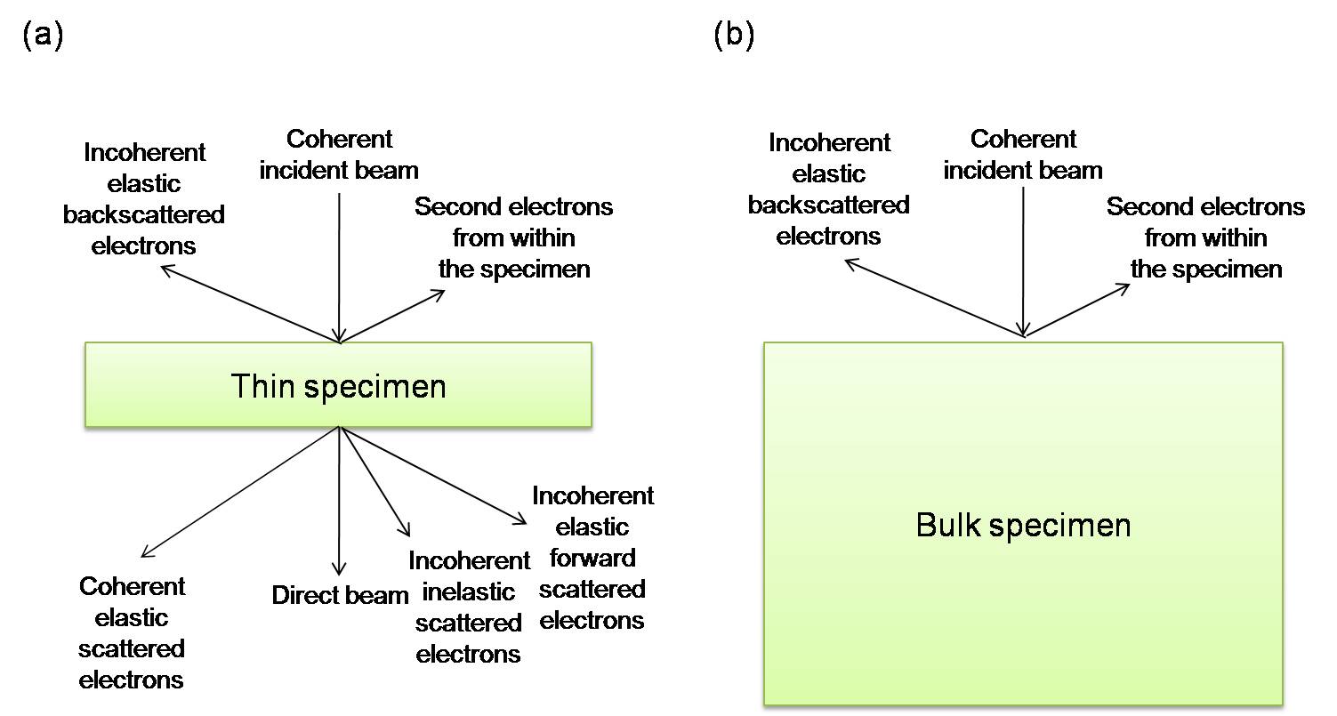
All scattering in the TEM specimen is often approximated as a single scattering event since it is the simplest process. If the specimen is very thin, this assumption will be reasonable enough. If the electron is scattered more than once, it is called ‘plural scattering.’ It is generally safe to assume single scattering occurs, unless the specimen is particularly thick. When the times of scattering increase, it is difficult to predict what will happen to the electron and to interpret the images and DPs. So, the principle is ‘thinner is better’, i.e., if we make thin enough specimens so that the single-scattering assumption is plausible, and the TEM research will be much easier.
In fact, forward scattering includes the direct beam, most elastic scattering, refraction, diffraction, particularly Bragg diffraction, and inelastic scattering. Because of forward scattering through the thin specimen, a DP or an image would be showed on the viewing screen, and an X-ray spectrum or an electron energy-loss spectrum can be detected outside the TEM column. However, backscattering still cannot be ignored, it is an important imagine mode in the SEM.
Limitations of TEM
Interpreting Transmission Images
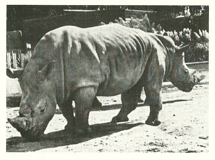
One significant problem that might encounter when TEM images are analyzed is that the TEM present us with 2D images of a 3D specimen, viewed in transmission. This problem can be illustrated by showing a picture of two rhinos side by side such that the head of one appears attached to the rear of the other (Figure \(\PageIndex{3}\)).
One aspect of this particular drawback is that a single TEM images has no depth sensitivity. There often is information about the top and bottom surfaces of the specimen, but this is not immediately apparent. There has been progress in overcoming this limitation, by the development of electron tomography, which uses a sequence of images taken at different angles. In addition, there has been improvement in specimen-holder design to permit full 360o rotation and, in combination with easy data storage and manipulation; nanotechnologists have begun to use this technique to look at complex 3D inorganic structures such as porous materials containing catalyst particles.
Electron Beam Damage
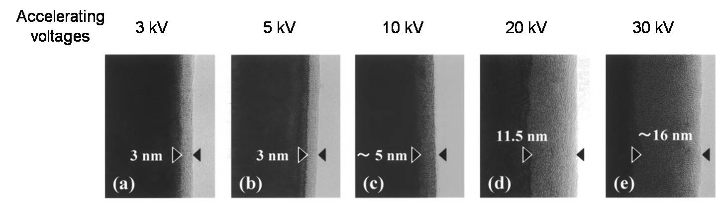
A detrimental effect of ionizing radiation is that it can damage the specimen, particularly polymers (and most organics) or certain minerals and ceramics. Some aspects of beam damage made worse at higher voltages. Figure \(\PageIndex{4}\) shows an area of a specimen damaged by high-energy electrons. However, the combination of more intense electron sources with more sensitive electron detectors, and the use computer enhancement of noisy images, can be used to minimize the total energy received by the sample.
Sample Preparation
The specimens under study have to be thin if any information is to be obtained using transmitted electrons in the TEM. For a sample to be transparent to electrons, the sample must be thin enough to transmit sufficient electrons such that enough intensity falls on the screen to give an image. This is a function of the electron energy and the average atomic number of the elements in the sample. Typically for 100 keV electrons, a specimen of aluminum alloy up to ~ 1 µm would be thin, while steel would be thin up to about several hundred nanometers. However, thinner is better and specimens < 100 nm should be used wherever possible.
The method to prepare the specimens for TEM depends on what information is required. In order to observe TEM images with high resolution, it is necessary to prepare thin films without introducing contamination or defects. For this purpose, it is important to select an appropriate specimen preparation method for each material, and to find an optimum condition for each method.
Crushing
A specimen can be crushed with an agate mortar and pestle. The flakes obtained are suspended in an organic solvent (e.g., acetone), and dispersed with a sonic bath or simply by stirring with a glass stick. Finally, the solvent containing the specimen flakes is dropped onto a grid. This method is limited to materials which tend to cleave (e.g., mica).
Electropolishing
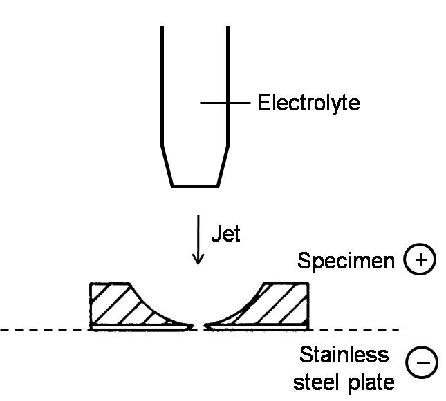
Slicing a bulk specimen into wafer plates of about 0.3 mm thickness by a fine cutter or a multi-wire saw. The wafer is further thinned mechanically down to about 0.1 mm in thickness. Electropolishing is performed in a specific electrolyte by supplying a direct current with the positive pole at the thin plate and the negative pole at a stainless steel plate. In order to avoid preferential polishing at the edge of the specimen, all the edges are cover with insulating paint. This is called the window method. The electropolishing is finished when there is a small hole in the plate with very thin regions around it (Figure \(\PageIndex{5}\)). This method is mainly used to prepare thin films of metals and alloys.
Chemical Polishing
Thinning is performed chemically, i.e., by dipping the specimen in a specific solution. As for electropolishing, a thin plate of 0.1~0.2 mm in thickness should be prepared in advance. If a small dimple is made in the center of the plate with a dimple grinder, a hole can be made by etching around the center while keeping the edge of the specimen relatively thick. This method is frequently used for thinning semiconductors such as silicon. As with electro-polishing, if the specimen is not washed properly after chemical etching, contamination such as an oxide layer forms on the surface.
Ultramicrotomy
Specimens of thin films or powders are usually fixed in an acrylic or epoxy resin and trimmed with a glass knife before being sliced with a diamond knife. This process is necessary so that the specimens in the resin can be sliced easily by a diamond knife. Acrylic resins are easily sliced and can be removed with chloroform after slicing. When using an acrylic resin, a gelatin capsule is used as a vessel. Epoxy resin takes less time to solidify than acrylic resins, and they remain strong under electron irradiation. This method has been used for preparing thin sections of biological specimens and sometimes for thin films of inorganic materials which are not too hard to cut.
Ion Milling
A thin plate (less than 0.1 mm) is prepared from a bulk specimen by using a diamond cutter and by mechanical thinning. Then, a disk 3 mm in diameter is made from the plate using a diamond knife or a ultrasonic cutter, and a dimple is formed in the center of the surface with a dimple grinder. If it is possible to thin the disk directly to 0.03 mm in thickness by mechanical thinning without using a dimple grinder, the disk should be strengthened by covering the edge with a metal ring. Ar ions are usually used for the sputtering, and the incidence angle against the disk specimen and the accelerating voltage are set as 10 - 20o and a few kilovolts, respectively. This method is widely used to obtain thin regions of ceramics and semiconductors in particular, and also for cross section of various multilayer films.
Focused Ion Beam (FIB)
This method was originally developed for the purpose of fixing semiconductor devices. In principle, ion beams are sharply focused on a small area, and the specimen in thinned very rapidly by sputtering. Usually Ga ions are used, with an accelerating voltage of about 30 kV and a current of about 10 A/cm2. The probe size is several tens of nanometers. This method is useful for specimens containing a boundary between different materials, where it may be difficult to homogeneously thin the boundary region by other methods such as ion milling.
Vacuum Evaporation
The specimen to be studied is set in a tungsten-coil or basket. Resistance heating is applied by an electric current passing through the coil or basket, and the specimen is melted, then evaporated (or sublimed), and finally deposited onto a substrate. The deposition process is usually carried under a pressure of 10-3-10-4 Pa, but in order to avoid surface contamination, a very high vacuum is necessary. A collodion film or cleaved rock salt is used as a substrate. Rock salt is especially useful in forming single crystals with a special orientation relationship between each crystal and the substrate. Salt is easily dissolved in water, and then the deposited films can be fixed on a grid. Recently, as an alternative to resistance heating, electron beam heating or an ion beam sputtering method has been used to prepare thin films of various alloys. This method is used for preparing homogeneous thin films of metals and alloys, and is also used for coating a specimen with the metal of alloy.
The Characteristics of the Grid
The types of TEM specimens that are prepared depend on what information is needed. For example, a self-supporting specimen is one where the whole specimen consists of one material (which may be a composite). Other specimens are supported on a grid or on a Cu washer with a single slot. Some grids are shown in Figure \(\PageIndex{6}\). Usually the specimen or grid will be 3 mm in diameter.
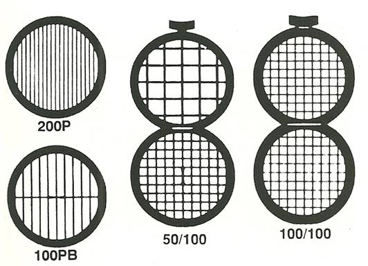
TEM specimen stage designs include airlocks to allow for insertion of the specimen holder into the vacuum with minimal increase in pressure in other areas of the microscope. The specimen holders are adapted to hold a standard size of grid upon which the sample is placed or a standard size of self-supporting specimen. Standard TEM grid sizes is a 3.05 mm diameter ring, with a thickness and mesh size ranging from a few to 100 µm. The sample is placed onto the inner meshed area having diameter of approximately 2.5 mm. The grid materials usually are copper, molybdenum, gold or platinum. This grid is placed into the sample holder which is paired with the specimen stage. A wide variety of designs of stages and holders exist, depending upon the type of experiment being performed. In addition to 3.05 mm grids, 2.3 mm grids are sometimes, if rarely, used. These grids were particularly used in the mineral sciences where a large degree of tilt can be required and where specimen material may be extremely rare. Electron transparent specimens have a thickness around 100 nm, but this value depends on the accelerating voltage.
Once inserted into a TEM, the sample is manipulated to allow study of the region of interest. To accommodate this, the TEM stage includes mechanisms for the translation of the sample in the XY plane of the sample, for Z height adjustment of the sample holder, and usually at least one rotation degree of freedom. Most TEMs provide the ability for two orthogonal rotation angles of movement with specialized holder designs called double-tilt sample holders.
A TEM stage is required to have the ability to hold a specimen and be manipulated to bring the region of interest into the path of the electron beam. As the TEM can operate over a wide range of magnifications, the stage must simultaneously be highly resistant to mechanical drift as low as a few nm/minute while being able to move several µm/minute, with repositioning accuracy on the order of nanometers.
Transmission Electron Microscopy Image for Multilayer-Nanomaterials
Although, TEMs can only provide 2D analysis for a 3D specimen; magnifications of 300,000 times can be routinely obtained for many materials making it an ideal methodfor the study of nanomaterials. Besides from the TEM images, darker areas of the image show that the sample is thicker or denser in these areas, so we can observe the different components and structures of the specimen by the difference of color. For investigating multilayer-nanomaterials, a TEM is usually the first choice, because not only does it provide a high resolution image for nanomaterials but also it can distinguish each layer within a nanostructured material.
Observations of Multilayer-nanomaterials
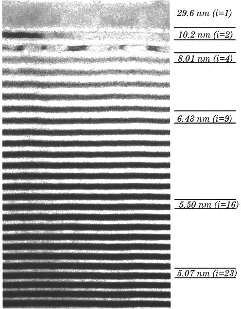
TEM was been used to analyze the depth-graded W/Si multilayer films. Multilayer films were grown on polished, 100 mm thick Si wafers by magnetron sputtering in argon gas. The individual tungsten and silicon layer thicknesses in periodic and depth-graded multilayers are adjusted by varying the computer-controlled rotational velocity of the substrate platen. The deposition times required to produce specific layer thicknesses were determined from detailed rate calibrations. Samples for TEM were prepared by focused ion beam milling at liquid N2 temperature to prevent any beam heating which might result in re-crystallization and/or re-growth of any amorphous or fine grained polycrystalline layers in the film.
TEM measurements were made using a JEOL-4000 high-resolution transmission electron microscope operating at 400 keV; this instrument has a point-to-point resolution of 0.16 nm. Large area cross-sectional images of a depth-graded multilayer film obtained under medium magnification (~100 kX) were acquired at high resolution. A cross-sectional TEM image showed 150 layers W/Si film with the thickness of layers in the range of 3.33 ~ 29.6 nm (Figure \(\PageIndex{7}\) shows a part of layers). The dark layers are tungsten and the light layers are silicon and they are separated by the thin amorphous W–Si interlayers (gray bands). By the high resolution of the TEM and the nature characteristics of the material, each layer can be distinguished clearly with their different darkness.
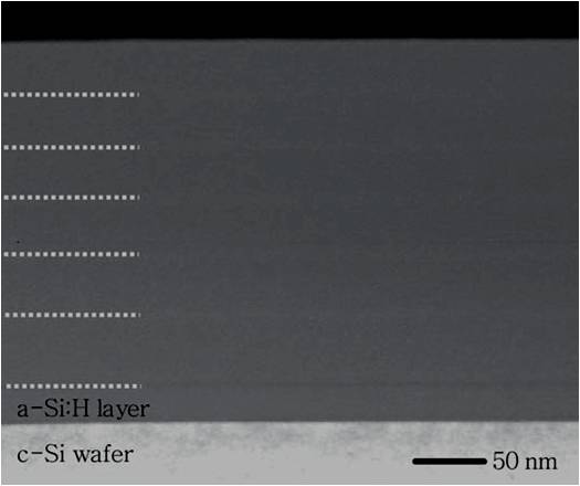
Not all kinds of multilayer nanomaterials can be observed clearly under TEM. A materials consist of pc-Si:H multilayers were prepared by a photo-assisted chemical vapor deposition (photo-CVD) using a low-pressure mercury lamp as an UV light source to dissociate the gases. The pc-Si:H multilayer included low H2-diluted a-Si:H sublayers (SL’s) and highly H2-diluted a-Si:H sublayers (SH’s). Control of the CVD gas flow (H2|SiH4) under continuous UV irradiation resulted in the deposition of multilayer films layer by layer.
For a TEM measurement, a 20 nm thick undiluted a-Si:H film on a c-Si wafer before the deposition of multilayer to prevent from any epitaxial growth. Figure \(\PageIndex{8}\) shows a cross-sectional TEM image of a six-cycled pc-Si:H multilayer specimen. The white dotted lines are used to emphasize the horizontal stripes, which have periodicity in the TEM image. As can be seen, there are no significant boundaries between SL and SH could be observed because all sublayers are prepared in H2 gas. In order to get the more accurate thickness of each sublayer, other measurements might be necessary.
TEM Imaging of Carbon Nanomaterials
Transmission electron microscopy (TEM) is a form of microscopy that uses an high energy electron beam (rather than optical light). A beam of electrons is transmitted through an ultra thin specimen, interacting with the specimen as it passes through. The image (formed from the interaction of the electrons with the sample) is magnified and focused onto an imaging device, such as a photographic film, a fluorescent screen,or detected by a CCD camera. In order to let the electrons pass through the specimen, the specimen has to be ultra thin, usually thinner than 10 nm.
The resolution of TEM is significantly higher than light microscopes. This is because the electron has a much smaller de Broglie wavelength than visible light (wavelength of 400~700 nm). Theoretically, the maximum resolution, d, has been limited by λ, the wavelength of the detecting source (light or electrons) and NA, the numerical aperture of the system.
\[ d\ = \frac{\lambda }{2n\ sin \alpha} \approx \frac{\lambda }{2NA} \label{8} \]
For high speed electrons (in TEM, electron velocity is close to the speed of light, c, so that the special theory of relativity has to be considered), the λe:
\[ \lambda _{e} =\ \frac{h}{\sqrt{2m_{0}E(1+E/2m_{0}c^{2})}} \label{9} \]
According to this formula, if we increase the energy of the detecting source, its wavelength will decrease, and we can get higher resolution. Today, the energy of electrons used can easily get to 200 keV, sometimes as high as 1 MeV, which means the resolution is good enough to investigate structure in sub-nanometer scale. Because the electrons is focused by several electrostatic and electromagnetic lenses, like the problems optical camera usually have, the image resolution is also limited by aberration, especially the spherical aberration called Cs. Equipped with a new generation of aberration correctors, transmission electron aberration-corrected microscope (TEAM) can overcome spherical aberration and get to half angstrom resolution.
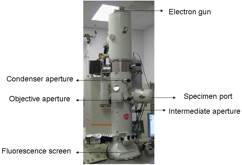
Although TEAM can easily get to atomic resolution, the first TEM invented by Ruska in April 1932 could hardly compete with optical microscope, with only 3.6×4.8 = 14.4 magnification. The primary problem was the electron irradiation damage to sample in poor vacuum system. After World War II, Ruska resumed his work in developing high resolution TEM. Finally, this work brought him the Nobel Prize in physics 1986. Since then, the general structure of TEM hasn’t changed too much as shown in Figure \(\PageIndex{9}\). The basic components in TEM are: electron gun, condenser system, objective lens (most important len in TEM which determines the final resolution), diffraction lens, projective lenses (all lens are inside the equipment column, between apertures), image recording system (used to be negative films, now is CCD cameras) and vacuum system.
The Family of Carbon Allotropes and Carbon Nanomaterials
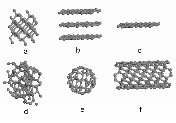
Common carbon allotropes include diamond, graphite, amorphrous C (a-C), fullerene (also known as buckyball), carbon nanotube (CNT, including single wall CNT and multi wall CNT), graphene. Most of them are chemically inert and have been found in nature. We can also define carbon as sp2 carbon (which is graphite), sp3 carbon (which is diamond) or hybrids of sp2 and sp3 carbon. As shown in Figure, (a) is the structure of diamond, (b) is the structure of graphite, (c) graphene is a single sheet of graphite, (d) is amorphous carbon, (e) is C60, and (f) is single wall nanotube. As for carbon nanomaterials, fullerene, CNT and graphene are the three most well investigated, due to their unique properties in both mechanics and electronics. Under TEM, these carbon nanomaterials will display three different projected images.
Atomic Structure of Carbon Nanomaterials under TEM
All carbon naomaterials can be investigated under TEM. Howerver, because of their difference in structure and shape, specific parts should be focused in order to obtain their atomic structure.
For C60, which has a diameter of only 1 nm, it is relatively difficult to suspend a sample over a lacey carbon grid (a common kind of TEM grid usually used for nanoparticles). Even if the C60 sits on a thin a-C film, it also has some focus problems since the surface profile variation might be larger than 1 nm. One way to solve this problem is to encapsulate the C60 into single wall CNTs, which is known as nano peapods. This method has two benefits:
CNT helps focus on C60. Single wall is aligned in a long distance (relative to C60). Once it is suspended on lacey carbon film, it is much easier to focus on it. Therefore, the C60 inside can also be caught by minor focus changes.
The CNT can protect C60 from electron irradiation. Intense high energy electrons can permanently change the structure of the CNT. For C60, which is more reactive than CNTs, it can not survive after exposing to high dose fast electrons.
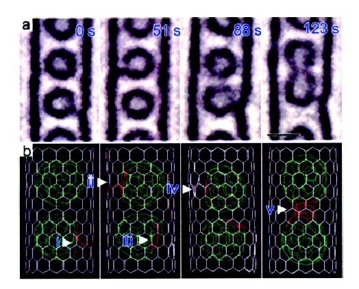
In studying CNT cages, C92 is observed as a small circle inside the walls of the CNT. While a majority of electron energy is absorbed by the CNT, the sample is still not irradiation-proof. Thus, as is seen in Figure \(\PageIndex{11}\), after a 123 s exposure, defects can be generated and two C92 fused into one new larger fullerene.
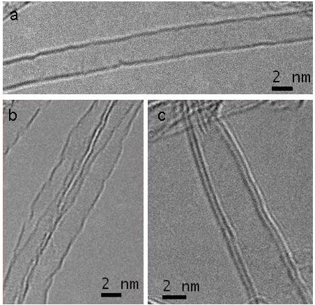
Although, the discovery of C60 was first confirmed by mass spectra rather than TEM. When it came to the discovery of CNTs, mass spectra was no longer useful because CNTs shows no individual peak in mass spectra since any sample contains a range of CNTs with different lengths and diameters. On the other hand, HRTEM can provide a clear image evidence of their existence. An example is shown in Figure \(\PageIndex{12}\).
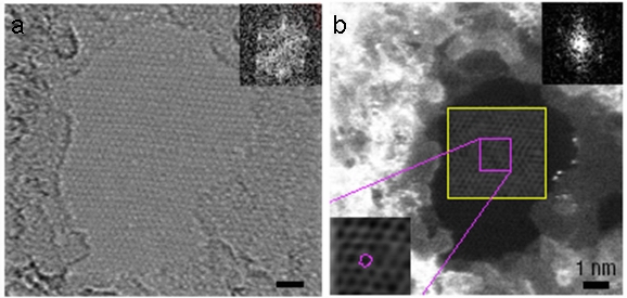
Graphene is a planar fullerene sheet. Until recently, Raman, AFM and optical microscopy (graphene on 300 nm SiO2 wafer) were the most convenient methods to characterize samples. However, in order to confirm graphene’s atomic structure and determine the difference between mono-layer and bi-layer, TEM is still a good option. In Figure \(\PageIndex{13}\), a monolayer suspended graphene is observed with its atomic structure clearly shown. Inset is the FFT of the TEM image, which can be used as a filter to get an optimized structure image. High angle annular dark field (HAADF) image usually gives better contrast for different particles on it. It is also sensitive with changes of thickness, which allows a determination of the number of graphene layers.
Graphene Stacking and Edges Direction
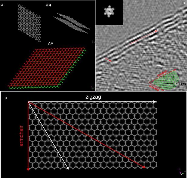
Like the situation in CNT, TEM image is a projected image. Therefore, even with exact count of edge lines, it is not possible to conclude that a sample is a single layer graphene or multi-layer. If folding graphene has AA stacking (one layer is superposed on the other), with a projected direction of [001], one image could not tell the thickness of graphene. In order to distinguish such a bilayer of graphene from a single layer of graphene, a series of tilting experiment must be done. Different stacking structures of graphene are shown in Figure \(\PageIndex{13}\) a.
Theoretically, graphene has the potential for interesting edge effects. Based upon its sp2 structure, its edge can be either that of a zigzag or armchair configuration. Each of these possess different electronic properties similar to that observed for CNTs. For both research and potential application, it is important to control the growth or cutting of graphene with one specific edge. But before testing its electronic properties, all the edges have to be identified, either by directly imaging with STM or by TEM. Detailed information of graphene edges can be obtained with HRTEM, simulated with fast fourier transform (FFT). In Figure \(\PageIndex{14}\) b, armchair directions are marked with red arrow respectively. A clear model in Figurec shows a 30 degree angle between zigzag edge and armchair edge.
Transmission Electron Energy Loss Spectroscopy
Electron energy loss spectroscopy (EELS) is a technique that measures electronic excitations within solid-state materials. When an electron beam with a narrow range of kinetic energy is directed at a material some electrons will be inelastically scattered, resulting in a kinetic energy loss. Electrons can be inelastically scattered from phonon excitations, plasmon excitations, interband transitions, or inner shell ionization. EELS measures the energy loss of these inelastically scattered electrons and can yield information on atomic composition, bonding, electronic properties of valance and conduction bands and surface properties. An example of atomic level composition mapping is shown in Figure \(\PageIndex{15}\) a. EELS has even been used to measure pressure and temperature within materials.
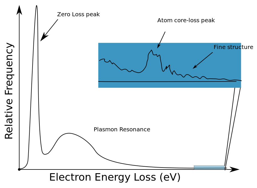
The EEl Spectrum
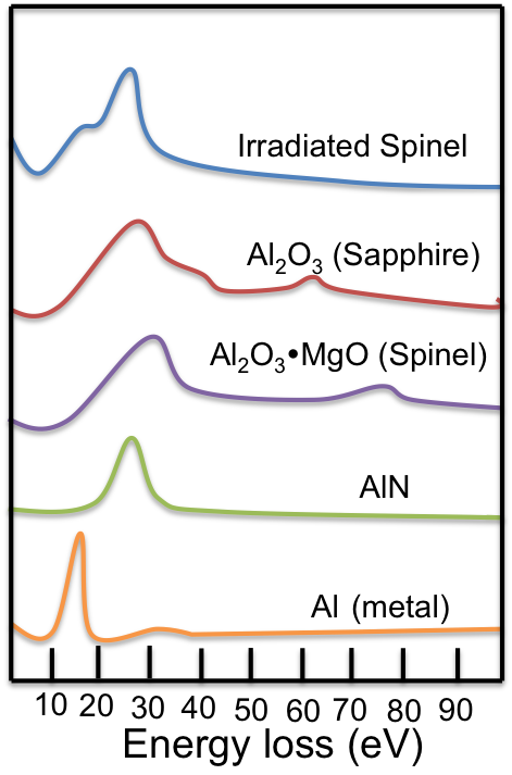
An idealized EEL spectrum is show in Figure \(\PageIndex{16}\). The most prominent feature of any EEL spectrum is the zero loss peak (ZLP). The ZLP is due to those electrons from the electron beam that do not inelastically scatter and reach the detector with their original kinetic energy; typically 100-300 keV. By definition the ZLP is set to 0 eV for further analysis and all signals arising from inelastically scatter electrons occur at >0 eV. The second largest feature is often the plasmon resonance - the collective excitation of conduction band electrons within a material. The plasmon resonance and other peaks attributed to weakly bound, or outer shell electrons, occur in the “low-loss” region of the spectrum. The low-loss regime is typically thought of as energy loss <50 eV, but this cut-off from low-loss to high-loss is arbitrary. Shown in the inset of Figure \(\PageIndex{16}\) is an edge from atom core-loss and further fine structure. Inner shell ionizations, represented by the core-loss peaks, are useful in determining elemental compositions as these peaks can act as fingerprints for specific elements. For example, if there is a peak at 532 eV in a EEL spectrum, there is a high probability that the sample contains a considerable amount of oxygen because this is known to be the energy needed to remove an inner shell electron from oxygen. This idea is further explored by looking at sudden changes in the bulk plasmon for aluminum in different chemical environments as shown in Figure \(\PageIndex{16}\).
Of course, there are several other techniques available for probing atomic compositions many of which are covered in this text. These include Energy dispersive X-ray spectroscopy, X-ray photoelectron spectroscopy, and Auger electron spectroscopy. Please reference these chapters thorough introduction to these techniques.
Electron Energy Loss Spectroscopy Versus Energy Dispersive X-ray Spectroscopy
As a technique EELS is most frequently compared to energy dispersive X-ray spectroscopy (EDX) also known as energy dispersive spectroscopy (EDS). Energy dispersive X-ray detectors are commonly found as analytical probes on both scanning and transmission electron microscopes. The popularity of EDS can be understood by recognizing the simplicity of compositional analysis using this technique. However, EELS data can offer complementary compositional analysis while also generally yielding further insight into the solid-state physics and chemistry in a system at the cost of a steeper learning curve. EDS and EELS spectra are both derived from the electronic excitations of materials, however, EELS probes the initial excitation while EDS looks at X-ray emissions from the decay of this excited state. As a result, EEL spectra investigate energy ranges from 0-3 keV while EDS spectra analyze a wider energy range from 1-40 keV. The difference in ranges makes EDS suited particularly well for heavy elements while EELS complements measurement elements lighter than Zn.
History and Implementation
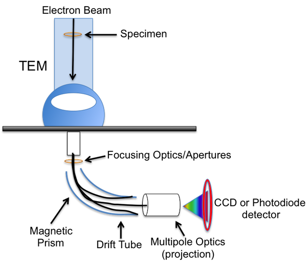
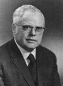
In the early 1940s, James Hillier (Figure \(\PageIndex{18}\)) and R.F. Baker were looking to develop a method for pairing the size, shape, and structure available from electron microscopes to a convenient method for “determining the composition of individual particles in a mixed specimen”. Their instrument, shown in Figure \(\PageIndex{19}\),reported in the Journal of Applied Physics in September 1994 was the first electron-optical instrument used to measure the velocity distribution in an electron beam transmitting through a sample.
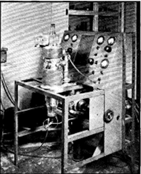
The instrument was built from a repurposed transmission electron microscope (TEM). It consisted of an electron source and three electromagnetic focusing lenses, standard for TEMs at the time, but also incorporated a magnetic deflecting lenses, which when turned on, would redirect the electrons 180° into a photographic plate. The electrons with varying kinetic energies dispersed across the photographic plate and could be correlated to the energy loss of each peak depending on position. In this groundbreaking work, Hillier and Baker were able to find the discrete energy loss corresponding to the K levels of both carbon and oxygen.
The vast majority of EEL spectrometers are found as secondary analyzers in transmission electron microscopes. It wasn’t until the 1990s when EELS became a widely used research tool because of advances in electron beam aberration correction and vacuum technologies. Today, EELS is capable of spatial resolutions down to the single atom level, and if the electron beam is monochromated energy resolution can be as low as 0.01eV. Figure \(\PageIndex{20}\) depicts the typical layout of an EEL spectrometer at the base of a TEM.