
21.3: Scanning Electron Microscopy
- Page ID
- 391929

\( \newcommand{\vecs}[1]{\overset { \scriptstyle \rightharpoonup} {\mathbf{#1}} } \)
\( \newcommand{\vecd}[1]{\overset{-\!-\!\rightharpoonup}{\vphantom{a}\smash {#1}}} \)
\( \newcommand{\dsum}{\displaystyle\sum\limits} \)
\( \newcommand{\dint}{\displaystyle\int\limits} \)
\( \newcommand{\dlim}{\displaystyle\lim\limits} \)
\( \newcommand{\id}{\mathrm{id}}\) \( \newcommand{\Span}{\mathrm{span}}\)
( \newcommand{\kernel}{\mathrm{null}\,}\) \( \newcommand{\range}{\mathrm{range}\,}\)
\( \newcommand{\RealPart}{\mathrm{Re}}\) \( \newcommand{\ImaginaryPart}{\mathrm{Im}}\)
\( \newcommand{\Argument}{\mathrm{Arg}}\) \( \newcommand{\norm}[1]{\| #1 \|}\)
\( \newcommand{\inner}[2]{\langle #1, #2 \rangle}\)
\( \newcommand{\Span}{\mathrm{span}}\)
\( \newcommand{\id}{\mathrm{id}}\)
\( \newcommand{\Span}{\mathrm{span}}\)
\( \newcommand{\kernel}{\mathrm{null}\,}\)
\( \newcommand{\range}{\mathrm{range}\,}\)
\( \newcommand{\RealPart}{\mathrm{Re}}\)
\( \newcommand{\ImaginaryPart}{\mathrm{Im}}\)
\( \newcommand{\Argument}{\mathrm{Arg}}\)
\( \newcommand{\norm}[1]{\| #1 \|}\)
\( \newcommand{\inner}[2]{\langle #1, #2 \rangle}\)
\( \newcommand{\Span}{\mathrm{span}}\) \( \newcommand{\AA}{\unicode[.8,0]{x212B}}\)
\( \newcommand{\vectorA}[1]{\vec{#1}} % arrow\)
\( \newcommand{\vectorAt}[1]{\vec{\text{#1}}} % arrow\)
\( \newcommand{\vectorB}[1]{\overset { \scriptstyle \rightharpoonup} {\mathbf{#1}} } \)
\( \newcommand{\vectorC}[1]{\textbf{#1}} \)
\( \newcommand{\vectorD}[1]{\overrightarrow{#1}} \)
\( \newcommand{\vectorDt}[1]{\overrightarrow{\text{#1}}} \)
\( \newcommand{\vectE}[1]{\overset{-\!-\!\rightharpoonup}{\vphantom{a}\smash{\mathbf {#1}}}} \)
\( \newcommand{\vecs}[1]{\overset { \scriptstyle \rightharpoonup} {\mathbf{#1}} } \)
\(\newcommand{\longvect}{\overrightarrow}\)
\( \newcommand{\vecd}[1]{\overset{-\!-\!\rightharpoonup}{\vphantom{a}\smash {#1}}} \)
\(\newcommand{\avec}{\mathbf a}\) \(\newcommand{\bvec}{\mathbf b}\) \(\newcommand{\cvec}{\mathbf c}\) \(\newcommand{\dvec}{\mathbf d}\) \(\newcommand{\dtil}{\widetilde{\mathbf d}}\) \(\newcommand{\evec}{\mathbf e}\) \(\newcommand{\fvec}{\mathbf f}\) \(\newcommand{\nvec}{\mathbf n}\) \(\newcommand{\pvec}{\mathbf p}\) \(\newcommand{\qvec}{\mathbf q}\) \(\newcommand{\svec}{\mathbf s}\) \(\newcommand{\tvec}{\mathbf t}\) \(\newcommand{\uvec}{\mathbf u}\) \(\newcommand{\vvec}{\mathbf v}\) \(\newcommand{\wvec}{\mathbf w}\) \(\newcommand{\xvec}{\mathbf x}\) \(\newcommand{\yvec}{\mathbf y}\) \(\newcommand{\zvec}{\mathbf z}\) \(\newcommand{\rvec}{\mathbf r}\) \(\newcommand{\mvec}{\mathbf m}\) \(\newcommand{\zerovec}{\mathbf 0}\) \(\newcommand{\onevec}{\mathbf 1}\) \(\newcommand{\real}{\mathbb R}\) \(\newcommand{\twovec}[2]{\left[\begin{array}{r}#1 \\ #2 \end{array}\right]}\) \(\newcommand{\ctwovec}[2]{\left[\begin{array}{c}#1 \\ #2 \end{array}\right]}\) \(\newcommand{\threevec}[3]{\left[\begin{array}{r}#1 \\ #2 \\ #3 \end{array}\right]}\) \(\newcommand{\cthreevec}[3]{\left[\begin{array}{c}#1 \\ #2 \\ #3 \end{array}\right]}\) \(\newcommand{\fourvec}[4]{\left[\begin{array}{r}#1 \\ #2 \\ #3 \\ #4 \end{array}\right]}\) \(\newcommand{\cfourvec}[4]{\left[\begin{array}{c}#1 \\ #2 \\ #3 \\ #4 \end{array}\right]}\) \(\newcommand{\fivevec}[5]{\left[\begin{array}{r}#1 \\ #2 \\ #3 \\ #4 \\ #5 \\ \end{array}\right]}\) \(\newcommand{\cfivevec}[5]{\left[\begin{array}{c}#1 \\ #2 \\ #3 \\ #4 \\ #5 \\ \end{array}\right]}\) \(\newcommand{\mattwo}[4]{\left[\begin{array}{rr}#1 \amp #2 \\ #3 \amp #4 \\ \end{array}\right]}\) \(\newcommand{\laspan}[1]{\text{Span}\{#1\}}\) \(\newcommand{\bcal}{\cal B}\) \(\newcommand{\ccal}{\cal C}\) \(\newcommand{\scal}{\cal S}\) \(\newcommand{\wcal}{\cal W}\) \(\newcommand{\ecal}{\cal E}\) \(\newcommand{\coords}[2]{\left\{#1\right\}_{#2}}\) \(\newcommand{\gray}[1]{\color{gray}{#1}}\) \(\newcommand{\lgray}[1]{\color{lightgray}{#1}}\) \(\newcommand{\rank}{\operatorname{rank}}\) \(\newcommand{\row}{\text{Row}}\) \(\newcommand{\col}{\text{Col}}\) \(\renewcommand{\row}{\text{Row}}\) \(\newcommand{\nul}{\text{Nul}}\) \(\newcommand{\var}{\text{Var}}\) \(\newcommand{\corr}{\text{corr}}\) \(\newcommand{\len}[1]{\left|#1\right|}\) \(\newcommand{\bbar}{\overline{\bvec}}\) \(\newcommand{\bhat}{\widehat{\bvec}}\) \(\newcommand{\bperp}{\bvec^\perp}\) \(\newcommand{\xhat}{\widehat{\xvec}}\) \(\newcommand{\vhat}{\widehat{\vvec}}\) \(\newcommand{\uhat}{\widehat{\uvec}}\) \(\newcommand{\what}{\widehat{\wvec}}\) \(\newcommand{\Sighat}{\widehat{\Sigma}}\) \(\newcommand{\lt}{<}\) \(\newcommand{\gt}{>}\) \(\newcommand{\amp}{&}\) \(\definecolor{fillinmathshade}{gray}{0.9}\)In optical microscopy we use photons to provide images of a sample. Although extraordinarily useful and powerful, the ability to resolve features in optical microscopy is limited by the source of light; in general, we can distinguish between two objects if they are separated by a distance that is greater than the wavelength of the photons being used. The maximum resolution for an optical microscope is about 0.2 µm (200 nm), which means we can use an optical microscope to view a human hair (20-200 µm), an eukaryotic cell (10-100 µm), a chloroplast (5-8 µm), and a mitochondrion (1-3 µm), but not a ribosome (0.01 µm-0.02 µm). In this section we will consider the electron microscope, which has a resolution limit of approximately 0.2 nm, or approximately \(1000 \times\) more than an optical microscope. In Section 21.4, we will examine two additional types of non-optical microscopy.
Instrumentation
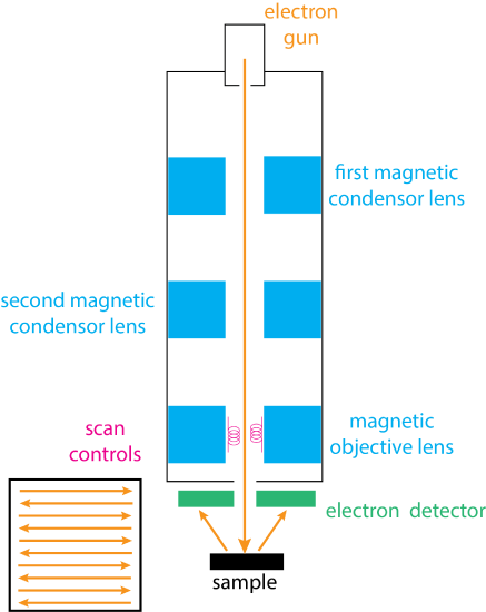
In scanning electron microscopy we raster a beam of high-energy electrons over a surface using a two-dimensional grid. Figure \(\PageIndex{1}\) shows the basic instrumental needs. The electron gun usually is just a simple tungsten wire that releases electrons when it is heated resistively. Other sources include solid-state crystals of lanthanum hexaboride (LaB6) or cerium hexaboride (CeB6) and the field emission gun, which uses a tungsten wire with a tip that has a radius of about 100 µm. Regardless of their source, these electrons are accelerated to an energy of 1-40 keV and passed through a series of lens that narrow and focus them into a beam with a diameter that falls within a range of 1 nm to 1000 nm (0.001 µm to 1 µm). A set of coiled scan controls deflects the electron beam in a raster pattern across the sample's surface (see inset at the bottom left of Figure \(\PageIndex{1}\)). An electron detector monitors the electrons that scatter back from the sample; the type of detector used varies with the type of emission from the sample that we choose to monitor—see the next sub-heading for types of emission—but typically are scintillation devices when monitoring electrons and energy-dispersive detectors when monitoring X-rays.
Interaction of Electron Beams With Solids
Figure \(\PageIndex{1}\) suggests that the only type of signal is the measurement of electrons that are scattered back toward the detector. The interaction between the electron beam and the sample, however creates a variety of signals, including both electrons and X-rays. Figure \(\PageIndex{2}\) illustrates the types of emission that follows from the interaction of the electron beam with the sample. The electron beam penetrates approximately 1-2 µm into the sample. As you might expect from the previous section on electron spectroscopy, the interaction of an electron beam with a sample results in the emission of some Auger electrons; these electrons come from a volume near the vacuum-sample interface. Of more importance are secondary electrons and backscattered electrons.
As the electron beam penetrates into the sample, the electrons undergo collisions with the sample's atoms. Some of these collisions are elastic in which the electron changes its direction, but retains its kinetic energy. With sufficient time, these electrons eventually undergo a collision in which they cross the sample-vacuum interface and exit the solid. These backscattered electrons are collected and passed along to the detector. Other electrons undergo inelastic collisions, losing kinetic energy and, eventually, become embedded in the sample. Backscattered electrons come from a depth as great as 50% of the depth to which the electron beam penetrates. Another source of electrons comes from a process in which the electron beam induces the ejection of electrons from the sample's conduction band. These secondary electrons are less numerous than backscattered electrons and they also come from a much shallower depth, typically 5-50 nm.
The electron beam also stimulates the release of X-rays, including the characteristic X-rays of the sample's elements, a broad continuum, and fluorescent X-ray emission. See Chapter 12 for more details about atomic X-ray emission.

As the electron beam is rastered across the sample, the intensity of the backscattered electrons from a specific position on the sample that reaches the detector is stored in the corresponding pixel on the instrument's monitor. The image created in this way is not an optical picture, but a digitized electronic reproduction of the sample's surface. The extent of magnification depends on the length of the detector's monitor relative to the length of a single scan across the sample; scanning a shorter distance results in a greater magnification. An optical microscope usually provides a maximum magnification of \(1000 \times\); an SEM can achieve a magnification of \(1,000,000 \times\).
Applications
Figure \(\PageIndex{3}\) shows four examples of applications of scanning electron microscopy for the measurement of particle size (upper left), for the evaluation of nanowires (upper right), for characterizing the channels in a microfluidic device (lower left), and for examining the tip of a cantilever and tip used for atomic force microscopy. Other applications include biological samples, films and coatings, fibers, and powders, to name a few.
