
21.4: Scanning Probe Microscopes
- Page ID
- 391931

\( \newcommand{\vecs}[1]{\overset { \scriptstyle \rightharpoonup} {\mathbf{#1}} } \)
\( \newcommand{\vecd}[1]{\overset{-\!-\!\rightharpoonup}{\vphantom{a}\smash {#1}}} \)
\( \newcommand{\id}{\mathrm{id}}\) \( \newcommand{\Span}{\mathrm{span}}\)
( \newcommand{\kernel}{\mathrm{null}\,}\) \( \newcommand{\range}{\mathrm{range}\,}\)
\( \newcommand{\RealPart}{\mathrm{Re}}\) \( \newcommand{\ImaginaryPart}{\mathrm{Im}}\)
\( \newcommand{\Argument}{\mathrm{Arg}}\) \( \newcommand{\norm}[1]{\| #1 \|}\)
\( \newcommand{\inner}[2]{\langle #1, #2 \rangle}\)
\( \newcommand{\Span}{\mathrm{span}}\)
\( \newcommand{\id}{\mathrm{id}}\)
\( \newcommand{\Span}{\mathrm{span}}\)
\( \newcommand{\kernel}{\mathrm{null}\,}\)
\( \newcommand{\range}{\mathrm{range}\,}\)
\( \newcommand{\RealPart}{\mathrm{Re}}\)
\( \newcommand{\ImaginaryPart}{\mathrm{Im}}\)
\( \newcommand{\Argument}{\mathrm{Arg}}\)
\( \newcommand{\norm}[1]{\| #1 \|}\)
\( \newcommand{\inner}[2]{\langle #1, #2 \rangle}\)
\( \newcommand{\Span}{\mathrm{span}}\) \( \newcommand{\AA}{\unicode[.8,0]{x212B}}\)
\( \newcommand{\vectorA}[1]{\vec{#1}} % arrow\)
\( \newcommand{\vectorAt}[1]{\vec{\text{#1}}} % arrow\)
\( \newcommand{\vectorB}[1]{\overset { \scriptstyle \rightharpoonup} {\mathbf{#1}} } \)
\( \newcommand{\vectorC}[1]{\textbf{#1}} \)
\( \newcommand{\vectorD}[1]{\overrightarrow{#1}} \)
\( \newcommand{\vectorDt}[1]{\overrightarrow{\text{#1}}} \)
\( \newcommand{\vectE}[1]{\overset{-\!-\!\rightharpoonup}{\vphantom{a}\smash{\mathbf {#1}}}} \)
\( \newcommand{\vecs}[1]{\overset { \scriptstyle \rightharpoonup} {\mathbf{#1}} } \)
\( \newcommand{\vecd}[1]{\overset{-\!-\!\rightharpoonup}{\vphantom{a}\smash {#1}}} \)
\(\newcommand{\avec}{\mathbf a}\) \(\newcommand{\bvec}{\mathbf b}\) \(\newcommand{\cvec}{\mathbf c}\) \(\newcommand{\dvec}{\mathbf d}\) \(\newcommand{\dtil}{\widetilde{\mathbf d}}\) \(\newcommand{\evec}{\mathbf e}\) \(\newcommand{\fvec}{\mathbf f}\) \(\newcommand{\nvec}{\mathbf n}\) \(\newcommand{\pvec}{\mathbf p}\) \(\newcommand{\qvec}{\mathbf q}\) \(\newcommand{\svec}{\mathbf s}\) \(\newcommand{\tvec}{\mathbf t}\) \(\newcommand{\uvec}{\mathbf u}\) \(\newcommand{\vvec}{\mathbf v}\) \(\newcommand{\wvec}{\mathbf w}\) \(\newcommand{\xvec}{\mathbf x}\) \(\newcommand{\yvec}{\mathbf y}\) \(\newcommand{\zvec}{\mathbf z}\) \(\newcommand{\rvec}{\mathbf r}\) \(\newcommand{\mvec}{\mathbf m}\) \(\newcommand{\zerovec}{\mathbf 0}\) \(\newcommand{\onevec}{\mathbf 1}\) \(\newcommand{\real}{\mathbb R}\) \(\newcommand{\twovec}[2]{\left[\begin{array}{r}#1 \\ #2 \end{array}\right]}\) \(\newcommand{\ctwovec}[2]{\left[\begin{array}{c}#1 \\ #2 \end{array}\right]}\) \(\newcommand{\threevec}[3]{\left[\begin{array}{r}#1 \\ #2 \\ #3 \end{array}\right]}\) \(\newcommand{\cthreevec}[3]{\left[\begin{array}{c}#1 \\ #2 \\ #3 \end{array}\right]}\) \(\newcommand{\fourvec}[4]{\left[\begin{array}{r}#1 \\ #2 \\ #3 \\ #4 \end{array}\right]}\) \(\newcommand{\cfourvec}[4]{\left[\begin{array}{c}#1 \\ #2 \\ #3 \\ #4 \end{array}\right]}\) \(\newcommand{\fivevec}[5]{\left[\begin{array}{r}#1 \\ #2 \\ #3 \\ #4 \\ #5 \\ \end{array}\right]}\) \(\newcommand{\cfivevec}[5]{\left[\begin{array}{c}#1 \\ #2 \\ #3 \\ #4 \\ #5 \\ \end{array}\right]}\) \(\newcommand{\mattwo}[4]{\left[\begin{array}{rr}#1 \amp #2 \\ #3 \amp #4 \\ \end{array}\right]}\) \(\newcommand{\laspan}[1]{\text{Span}\{#1\}}\) \(\newcommand{\bcal}{\cal B}\) \(\newcommand{\ccal}{\cal C}\) \(\newcommand{\scal}{\cal S}\) \(\newcommand{\wcal}{\cal W}\) \(\newcommand{\ecal}{\cal E}\) \(\newcommand{\coords}[2]{\left\{#1\right\}_{#2}}\) \(\newcommand{\gray}[1]{\color{gray}{#1}}\) \(\newcommand{\lgray}[1]{\color{lightgray}{#1}}\) \(\newcommand{\rank}{\operatorname{rank}}\) \(\newcommand{\row}{\text{Row}}\) \(\newcommand{\col}{\text{Col}}\) \(\renewcommand{\row}{\text{Row}}\) \(\newcommand{\nul}{\text{Nul}}\) \(\newcommand{\var}{\text{Var}}\) \(\newcommand{\corr}{\text{corr}}\) \(\newcommand{\len}[1]{\left|#1\right|}\) \(\newcommand{\bbar}{\overline{\bvec}}\) \(\newcommand{\bhat}{\widehat{\bvec}}\) \(\newcommand{\bperp}{\bvec^\perp}\) \(\newcommand{\xhat}{\widehat{\xvec}}\) \(\newcommand{\vhat}{\widehat{\vvec}}\) \(\newcommand{\uhat}{\widehat{\uvec}}\) \(\newcommand{\what}{\widehat{\wvec}}\) \(\newcommand{\Sighat}{\widehat{\Sigma}}\) \(\newcommand{\lt}{<}\) \(\newcommand{\gt}{>}\) \(\newcommand{\amp}{&}\) \(\definecolor{fillinmathshade}{gray}{0.9}\)in the last section we considered how we can image a surface using an electron beam. In this section we consider a very different approach to developing an image of a surface, one in which we bring a probe close to the surface and examine how the probe interacts with the surface. One advantage of this approach is that the interaction between the probe and the surface can include attraction and repulsion, which opens up a third dimension to the image.
Scanning Tunneling Microscope (STM)
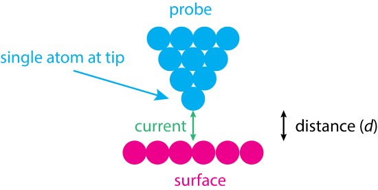
In the scanning tunneling microscope we take advantage of the ability of a current to pass through the gap between the tip of a conducting probe and a conducting sample when the probe and the sample are held at different potentials. Figure \(\PageIndex{1}\) shows the basic arrangement in which the probe has, ideally, a single atom at its tip. The tunneling current, \(I_t\) is given by
\[I_t = V e^{-Cd} \label{stm1} \]
where \(V\) is the applied voltage, \(d\) is the distance between the probe's tip and the sample, and \(C\) is a constant whose value depends upon the composition of the probe and the sample. The exponential decrease in the tunneling current with distance means that a small change in the position of probe's tip relative to the sample results in a significant change in the signal, providing vertical resolution on the order of 0.1 nm. Probes are fashioned using tungsten wires or platinum-iridium wires.
Scanning tunneling microscopy images are created by moving the probe back-and-forth across the sample while measuring the current. The signal is acquired in one of two modes: constant current or constant height. In constant current mode, the probe's tip is brought near the surface and the current measured, which establishes a setpoint. As the probe moves across the sample, it is raised or lowered to maintain the setpoint current. The result is measure of the distance, \(d\), between the probe's tip and the sample along the z-axis as a function of the xy position of the probe's tip. In constant height mode, the distance, \(d\), between the probe's tip and the sample is held constant, and the current, \(I_t\), is measured as a function of the xy position of the probe's tip. Constant height mode allows for faster data acquisition, but is limited to samples that have flat surfaces.
Positioning of the sample and the probe's tip relative to each other is accomplished by either moving the probe or moving the sample. In either case, the control of movement in accomplished using a piezoelectric scanner. A piezoelectric material, as shown in Figure \(\PageIndex{2}\) experiences a change in its length when a dc potential is applied across its sides, either extending its length or contracting its length.
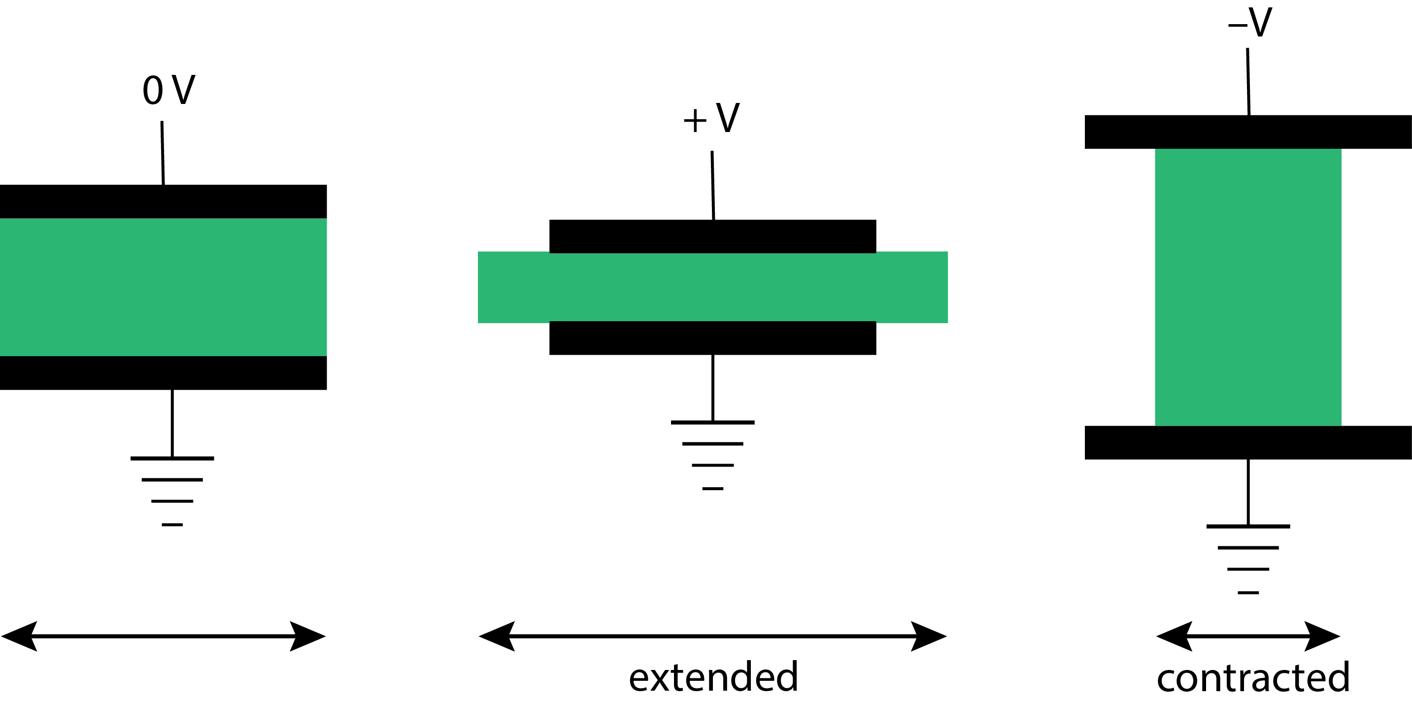
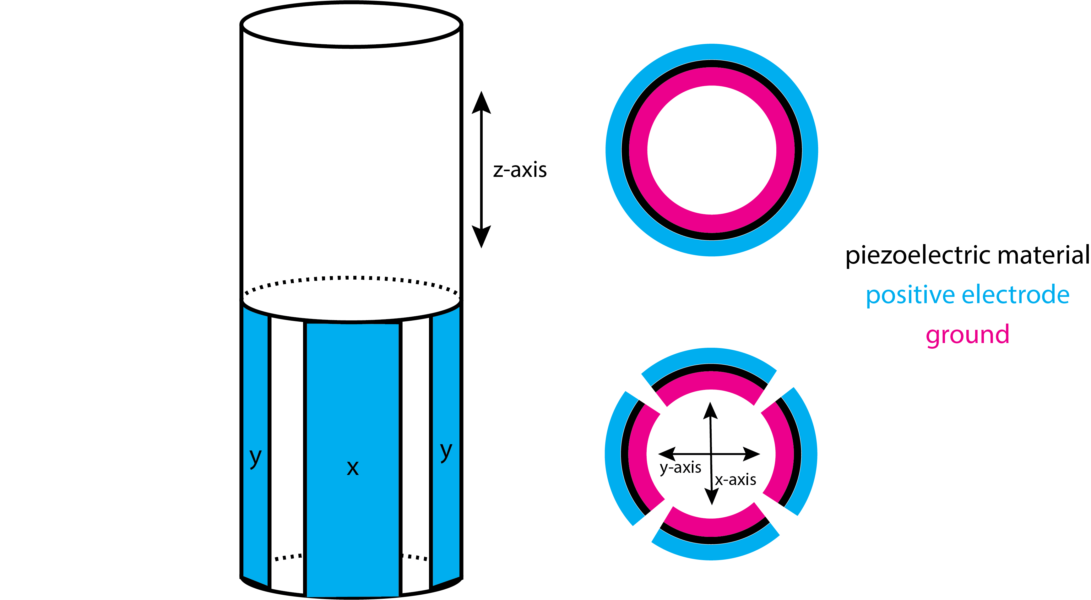
Figure \(\PageIndex{3}\) shows a configuration of cylindrical piezoelectric scanner in which the cylinder's upper half controls movement along the z-axis, and the cylinder's lower half is used to control movement along the x-axis, the y-axis, or both.
One limitation of STM is that the sample must be conductive. It is possible to image a non-conducting sample if it first coated with a conductive material, such as gold, although such coatings can mask surface features.
Atomic Force Microscope (AFM)
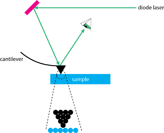
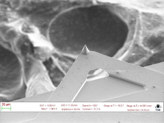
Unlike the scanning tunneling microscope, the atomic force microscope does not require a conducting sample and imaging is achieved without a current flowing between the sample and the tip of the probe. Instead, as shown in Figure \(\PageIndex{4}\), the probe is attached to the end of a flexible cantilever. The tip of the probe (see photograph in Figure \(\PageIndex{3}\)) is pyramidal in shape and extends about 10 µm from its base on the cantilever. The tip of the probe has a diameter on the order of 10 nm and is made of silicon, Si, or silicon nitride, Si3N4. The cantilever typically is 100-500 µm in length. The probe is scanned across the sample's surface and the position of the probe relative to the surface is determined by reflecting the beam from a diode laser off the probe-end of the cantilever to a detector.
The force in atomic force is the interaction between the probe's tip and the sample, which may be a force of attraction or a force of repulsion. When the probe's tip is in contact with the sample—known as contact mode—there is a force of repulsion between them. Because the cantilever has a smaller force constant than the atoms in the probe's tip, the cantilever bends. Moving the sample stage to maintain a constant deflection of the laser off of the cantilever provides an image of the sample's surface. Contact mode allows for rapid scanning and work well for samples with rough surfaces, although it may damage samples with softer surfaces.
In non-contact mode, the probe's tip is brought close to the sample's surface, but not allowed to come into contact with it. The cantilever is place into an oscillatory motion. The amplitude of this oscillation is proportional to the force of attraction between the probe's tip and the sample, which varies with the distance between the probe's tip and the sample. Moving the sample stage to maintain a constant oscillation provides an image of the sample's surface. Non-contact mode AFM generally provides lower resolution images, but is less damaging to the sample.
A third mode for collecting data is called intermittent or tapping mode. In this mode the cantilever is set to oscillate at its resonant frequency with the probe's tip coming into contact with the sample's surface when it reaches the bottom of the cantilever's oscillation. The frequency of the oscillation is sensitive to the distance between the probe's tip and the sample. Moving the sample stage to maintain the resonant frequency provides an image of the sample's surface.
You can view a gallery of scanning tunneling microscopy images here, and a gallery of atomic force microscopy images here.