
5.5: Bonding in Metals and Semicondoctors
- Page ID
- 326189
Band Theory
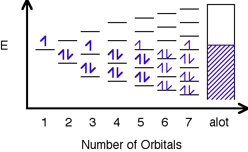
Band theory was developed with some help from the knowledge gained during the quantum revolution in science. In 1928, Felix Bloch had the idea to take the quantum theory and apply it to solids. In 1927, Walter Heitler and Fritz London discovered bands- very closely spaced orbitals with not much difference in energy. One way to conceptualize band theory is to view is as an extension of molecular orbital theory where the number of atomic orbitals mixed is increased to an infinite number and the energy difference between the molecular orbitals formed approaches 0 (Figure \(\PageIndex{1}\)).
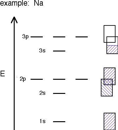
Different metals will produce different combinations of filled and half filled bands depending on their valence electron configuration. Sodium's bands are shown in Figure \(\PageIndex{2}\). As you can see, bands may overlap each other (the bands are shown askew to be able to tell the difference between different bands). The lowest unoccupied band is called the conduction band, and the highest occupied band is called the valence band.
Bands will follow a trend as you go across a period:
- In Na, the 3s band is 1/2 full.
- In Mg, the 3s band is full.
- In Al, the 3s band is full and the 3p band is 1/2 full... and so on.
In order for the material to conduct electricity, electrons should be in the conduction band where they are able to move freely through the material. The probability of finding an electron in the conduction band is shown by the equation:
\[ P= \dfrac{1}{e^{ \frac{\Delta E}{k_bT}}+1} \]
The ∆E in the equation stands for the energy gap between the valence and conduction bands. kb is the Boltzmann constant and T is temperature in K. That equation and the table below show that the larger the band gap between the valence band and the conduction band, the less likely electrons are to be found in the conduction band. This is because they don't have sufficient energy to make the jump up to the conduction band.
Table \(\PageIndex{1}\): Band Gaps and Conduction Band Electron Densities for Group 4 Elements
| ELEMENT | ∆E(kJ/mol) of energy gap | # of electrons/cm^3 in conduction band | material type |
|---|---|---|---|
| C (diamond) | 524 | 10-27 | insulator |
| Si | 117 | 109 | semiconductor |
| Ge | 66 | 1013 | semiconductor |
Conductors, Insulators and Semiconductors
The conductivity of materials is directly related to the band gap and the probability of having electrons in the conduction band. Materials can be divided into three classes based on their band gaps (Figure \(\PageIndex{3}\)).
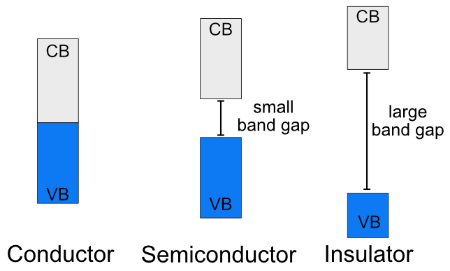 Figure \(\PageIndex{3}\): Illustration of the energy difference between the valence band (VB) and conduction band (CB) in conductors, semiconductors and insulators. (CC BY-NC-SA; Catherine McCusker)
Conductors
Conductors have no band gap between their valence and conduction bands, since they overlap. There is no barrier for electrons to move from the valence to conduction band. Electrons can move freely through the material, which makes it able to conduct electricity. When the temperature of a conductor increases, the resistivity increases (and the conductivity decreases). Conductivity and resistivity are inversely proportional to each other. When conductivity is low, resistivity is high. When resistivity is low, conductivity is high. Since conductivity is the measure of how easily electricity flows, electrical resistivity measures how much a material resists the flow of electricity. As electrons move through a material, they come into contact with nuclei in the material. Collisions slow the electrons down. Each collision increases the resistivity of the material, and as temperature increases the electron are more likely to have collisions.
Insulators
Insulators have a large band gap between the valence and conduction bands. In insulators electrons do not have sufficient energy to jump from the valence band to the conduction band and the probability of finding an electron in the conduction band approaches 0. An insulator material won't conduct any electricity at any temperature.
Semiconductors
Semiconductors are an intermediate between conductors and insulators. They have a small energy gap between the valence band and the conduction band. Some electrons have sufficient energy that they can make the jump up to the conduction band. Semiconductors can conduct electricity, but not as easily as conductors. The probability of finding electrons in the conduction band of a semiconductor, and therefore it's ability to conduct electricity, will vary with the band gap and the temperature. Unlike conductors, semiconductors are more conductive at higher temperatures because more electrons have the energy to jump into the conduction band. There are two types of semiconductors: intrinsic and extrinsic.
Intrinsic Semiconductors
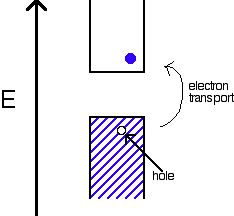
An intrinsic semiconductor is a pure material with a small band gap. For every electron that jumps into the conduction band, the missing electron will generate a hole that can move freely in the valence band. Both conduction band electrons and valence band holes can contribute to conducting electricity. The number of holes will equal the number of electrons that have jumped.
Extrinsic Semiconductors
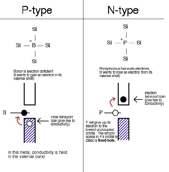
Extrinsic semiconductors are not good conductors in their pure forms, they have larger band gaps than intrinsic semiconductors. In extrinsic semiconductors, the conductivity is controlled by purposefully adding small amounts of impurities to the material. This process is called doping. Doping, or adding impurities to the lattice can change the electrical conductivity of the lattice and therefore vary the efficiency of the semiconductor. In extrinsic semiconductors, the number of valence band holes will not equal the number of conduction band electrons. Silicon is one of the most common extrinsic semiconductors. If silicon is doped with an atom with fewer electron, such as boron, electron from the silicon valence band can hop to the boron atoms, leaving holes in the valence band to conduct electricity. If silicon is doped with an atom with more electrons, such as phosphorus, the extra electron from the phosphorus atoms can jump into the silicon conduction band.
Exercise \(\PageIndex{1}\)
Describe the difference between a valence band and a conduction band
- Answer
-
The valence band is the highest band with electrons in it, the equivalent of the HOMO in MO theory. The conduction band is the highest band with no electrons in it, the equivalent of the LUMO in MO theory.
Exercise \(\PageIndex{2}\)
A conductor material and a semiconductor material have the same conductivity at 100 K. Which will be more conductive when the temperature is increased to 200 K?
- Answer
-
The conductivity of conductors will decrease as the temperature increases and the conductivity of semiconductors will increase as the temperature increases. Therefore at higher temperature the semiconductor material will have higher conductivity.
References
- Levy, Peter M., and Shufeng Zhang. "Electrical Conductivity of Magnetic Multilayered Structures." Physical Review Letters 65.13 (1990): 1643-646. Print.
- Petrucci, Harwood, Herring, Madura. GENERAL CHEMISTRY Principles and Modern Applications 9th Edition. Macmillan Publishing Co: New Jersey. 1989.
- Moore, John T. Chemistry Made Simple. Random House Inc: New York. 2004.
Contributors and Attributions
- Michael Ford (UCD) and Alexandra Christman (UCD)
- Sierra Blair (UCD)
Jim Clark (Chemguide.co.uk)