7.12: Applications for Silica Thin Films
- Page ID
- 212901
\( \newcommand{\vecs}[1]{\overset { \scriptstyle \rightharpoonup} {\mathbf{#1}} } \)
\( \newcommand{\vecd}[1]{\overset{-\!-\!\rightharpoonup}{\vphantom{a}\smash {#1}}} \)
\( \newcommand{\id}{\mathrm{id}}\) \( \newcommand{\Span}{\mathrm{span}}\)
( \newcommand{\kernel}{\mathrm{null}\,}\) \( \newcommand{\range}{\mathrm{range}\,}\)
\( \newcommand{\RealPart}{\mathrm{Re}}\) \( \newcommand{\ImaginaryPart}{\mathrm{Im}}\)
\( \newcommand{\Argument}{\mathrm{Arg}}\) \( \newcommand{\norm}[1]{\| #1 \|}\)
\( \newcommand{\inner}[2]{\langle #1, #2 \rangle}\)
\( \newcommand{\Span}{\mathrm{span}}\)
\( \newcommand{\id}{\mathrm{id}}\)
\( \newcommand{\Span}{\mathrm{span}}\)
\( \newcommand{\kernel}{\mathrm{null}\,}\)
\( \newcommand{\range}{\mathrm{range}\,}\)
\( \newcommand{\RealPart}{\mathrm{Re}}\)
\( \newcommand{\ImaginaryPart}{\mathrm{Im}}\)
\( \newcommand{\Argument}{\mathrm{Arg}}\)
\( \newcommand{\norm}[1]{\| #1 \|}\)
\( \newcommand{\inner}[2]{\langle #1, #2 \rangle}\)
\( \newcommand{\Span}{\mathrm{span}}\) \( \newcommand{\AA}{\unicode[.8,0]{x212B}}\)
\( \newcommand{\vectorA}[1]{\vec{#1}} % arrow\)
\( \newcommand{\vectorAt}[1]{\vec{\text{#1}}} % arrow\)
\( \newcommand{\vectorB}[1]{\overset { \scriptstyle \rightharpoonup} {\mathbf{#1}} } \)
\( \newcommand{\vectorC}[1]{\textbf{#1}} \)
\( \newcommand{\vectorD}[1]{\overrightarrow{#1}} \)
\( \newcommand{\vectorDt}[1]{\overrightarrow{\text{#1}}} \)
\( \newcommand{\vectE}[1]{\overset{-\!-\!\rightharpoonup}{\vphantom{a}\smash{\mathbf {#1}}}} \)
\( \newcommand{\vecs}[1]{\overset { \scriptstyle \rightharpoonup} {\mathbf{#1}} } \)
\( \newcommand{\vecd}[1]{\overset{-\!-\!\rightharpoonup}{\vphantom{a}\smash {#1}}} \)
\(\newcommand{\avec}{\mathbf a}\) \(\newcommand{\bvec}{\mathbf b}\) \(\newcommand{\cvec}{\mathbf c}\) \(\newcommand{\dvec}{\mathbf d}\) \(\newcommand{\dtil}{\widetilde{\mathbf d}}\) \(\newcommand{\evec}{\mathbf e}\) \(\newcommand{\fvec}{\mathbf f}\) \(\newcommand{\nvec}{\mathbf n}\) \(\newcommand{\pvec}{\mathbf p}\) \(\newcommand{\qvec}{\mathbf q}\) \(\newcommand{\svec}{\mathbf s}\) \(\newcommand{\tvec}{\mathbf t}\) \(\newcommand{\uvec}{\mathbf u}\) \(\newcommand{\vvec}{\mathbf v}\) \(\newcommand{\wvec}{\mathbf w}\) \(\newcommand{\xvec}{\mathbf x}\) \(\newcommand{\yvec}{\mathbf y}\) \(\newcommand{\zvec}{\mathbf z}\) \(\newcommand{\rvec}{\mathbf r}\) \(\newcommand{\mvec}{\mathbf m}\) \(\newcommand{\zerovec}{\mathbf 0}\) \(\newcommand{\onevec}{\mathbf 1}\) \(\newcommand{\real}{\mathbb R}\) \(\newcommand{\twovec}[2]{\left[\begin{array}{r}#1 \\ #2 \end{array}\right]}\) \(\newcommand{\ctwovec}[2]{\left[\begin{array}{c}#1 \\ #2 \end{array}\right]}\) \(\newcommand{\threevec}[3]{\left[\begin{array}{r}#1 \\ #2 \\ #3 \end{array}\right]}\) \(\newcommand{\cthreevec}[3]{\left[\begin{array}{c}#1 \\ #2 \\ #3 \end{array}\right]}\) \(\newcommand{\fourvec}[4]{\left[\begin{array}{r}#1 \\ #2 \\ #3 \\ #4 \end{array}\right]}\) \(\newcommand{\cfourvec}[4]{\left[\begin{array}{c}#1 \\ #2 \\ #3 \\ #4 \end{array}\right]}\) \(\newcommand{\fivevec}[5]{\left[\begin{array}{r}#1 \\ #2 \\ #3 \\ #4 \\ #5 \\ \end{array}\right]}\) \(\newcommand{\cfivevec}[5]{\left[\begin{array}{c}#1 \\ #2 \\ #3 \\ #4 \\ #5 \\ \end{array}\right]}\) \(\newcommand{\mattwo}[4]{\left[\begin{array}{rr}#1 \amp #2 \\ #3 \amp #4 \\ \end{array}\right]}\) \(\newcommand{\laspan}[1]{\text{Span}\{#1\}}\) \(\newcommand{\bcal}{\cal B}\) \(\newcommand{\ccal}{\cal C}\) \(\newcommand{\scal}{\cal S}\) \(\newcommand{\wcal}{\cal W}\) \(\newcommand{\ecal}{\cal E}\) \(\newcommand{\coords}[2]{\left\{#1\right\}_{#2}}\) \(\newcommand{\gray}[1]{\color{gray}{#1}}\) \(\newcommand{\lgray}[1]{\color{lightgray}{#1}}\) \(\newcommand{\rank}{\operatorname{rank}}\) \(\newcommand{\row}{\text{Row}}\) \(\newcommand{\col}{\text{Col}}\) \(\renewcommand{\row}{\text{Row}}\) \(\newcommand{\nul}{\text{Nul}}\) \(\newcommand{\var}{\text{Var}}\) \(\newcommand{\corr}{\text{corr}}\) \(\newcommand{\len}[1]{\left|#1\right|}\) \(\newcommand{\bbar}{\overline{\bvec}}\) \(\newcommand{\bhat}{\widehat{\bvec}}\) \(\newcommand{\bperp}{\bvec^\perp}\) \(\newcommand{\xhat}{\widehat{\xvec}}\) \(\newcommand{\vhat}{\widehat{\vvec}}\) \(\newcommand{\uhat}{\widehat{\uvec}}\) \(\newcommand{\what}{\widehat{\wvec}}\) \(\newcommand{\Sighat}{\widehat{\Sigma}}\) \(\newcommand{\lt}{<}\) \(\newcommand{\gt}{>}\) \(\newcommand{\amp}{&}\) \(\definecolor{fillinmathshade}{gray}{0.9}\)Introduction
While the physical properties of silica make it suitable for use in protective and optical coating applications, the biggest application of insulating SiO2 thin films is undoubtedly in semiconductor devices, in which the insulator performs a number of specific tasks, including: surface passivation, field effect transistor (FET) gate layer, isolation layers, planarization and packaging.
The term insulator generally refers to a material that exhibits low thermal or electrical conductivity; electrically insulating materials are also called dielectrics. It is in regard to the high resistance to the flow of an electric current that SiO2 thin films are of the greatest commercial importance. The dielectric constant (ε) is a measure of a dielectric materials ability to store charge, and is characterized by the electrostatic energy stored per unit volume across a unit potential gradient. The magnitude of ε is an indication of the degree of polarization or charge displacement within a material. The dielectric constant for air is 1, and for ionic solids is generally in the range of 5 - 10. Dielectric constants are defined as the ratio of the material’s capacitance to that of air, i.e., (7.12.1). The dielectric constant for silicon dioxide ranges from 3.9 to 4.9, for thermally and plasma CVD grown films, respectively.
\[ \epsilon \text{ = } \dfrac{\text{C}_{\text{material}}}{\text{C}_{\text{air}}}\]
An insulating layer is a film or deposited layer of dielectric material separating or covering conductive layers. Ideally, in these application an insulating material should have a surface resistivity of greater than 1013 Ω/cm2 or a volume resistivity of greater than 1011 Ω.cm. However, for some applications, lower values are acceptable; an electrical insulator is generally accepted to have a resistivity greater than 105 Ω.cm. CVD SiO2 thin films have a resistivity of 106 - 1016 Ω.cm, depending on the film growth method.
As a consequence of its dielectric properties SiO2, and related silicas, are used for isolating conducting layers, to facilitate the diffusion of dopants from doped oxides, as diffusion and ion implantation masks, capping doped films to prevent loss of dopant, for gettering impurities, for protection against moisture and oxidation, and for electronic passivation. Of the many methods used for the deposition of thin films, chemical vapor deposition (CVD) is most often used for semiconductor processing. In order to appreciate the unique problems associated with the CVD of insulating SiO2 thin films it is worth first reviewing some of their applications. Summarized below are three areas of greatest importance to the fabrication of contemporary semiconductor devices: isolation and gate insulation, passivation, and planarization.
Device isolation and gate insulation
A microcircuit may be described as a collection of devices each consisting of "an assembly of active and passive components, interconnected within a monolithic block of semiconducting material". Each device is required to be isolated from adjacent devices in order to allow for maximum efficiency of the overall circuit. Furthermore within a device, contacts must also be electrically isolated. While there are a number of methods for isolating individual devices within a circuit (reverse-biased junctions, mesa isolation, use of semi-insulating substrates, and oxide isolation), the isolation of the active components in a single device is almost exclusively accomplished by the deposition of an insulator.
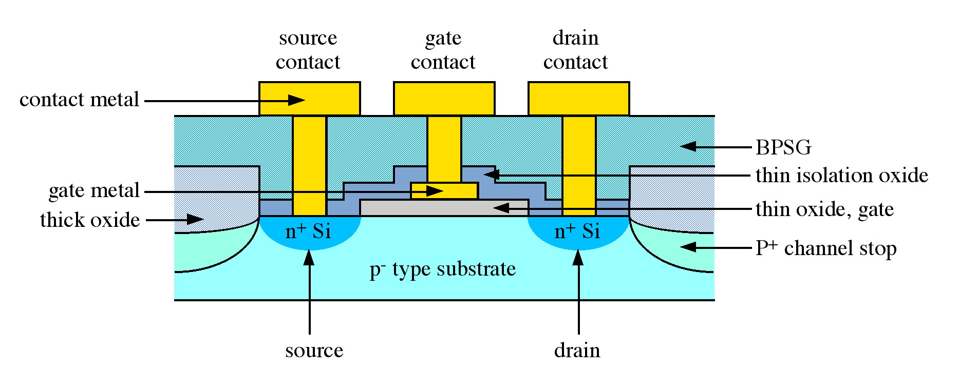
In Figure is shown a schematic representation of a silicon MOSFET (metal-oxide-semiconductor field effect transistor). The MOSFET is the basic component of silicon-CMOS (complimentary metal-oxide-semiconductor) circuits which, in turn, form the basis for logic circuits, such as those used in the CPU (central processing unit) of a modern personal computer. It can be seen that the MOSFET is isolated from adjacent devices by a reverse-biased junction (p+-channel stop) and a thick oxide layer. The gate, source and drain contact are electrically isolated from each other by a thin insulating oxide. A similar scheme is used for the isolation of the collector from both the base and the emitter in bipolar transistor devices.

As a transistor, a MOSFET has many advantages over alternate designs. The key advantage is low power dissipation resulting from the high impedance of the device. This is a result of the thin insulation layer between the channel (region between source and drain) and the gate contact, see Figure \(\PageIndex{1}\). The presence of an insulating gate is characteristic of a general class of devices called MISFETs (metal-insulator-semiconductor field effect transistor). MOSFETs are a subset of MISFETs where the insulator is specifically an oxide, e.g., in the case of a silicon MISFET device the insulator is SiO2, hence MOSFET. It is the fabrication of MOSFET circuits that has allowed silicon technology to dominate digital electronics (logic circuits). However, increases in computing power and speed require a constant reduction in device size and increased complexity in device architecture.
Passivation
Passivation is often defined as a process whereby a film is grown on the surface of a semiconductor to either (a) chemically protect it from the environment, or (b) provide electronic stabilization of the surface.
From the earliest days of solid state electronics it has been recognized that the presence or absence of surface states plays a decisive role in the usefulness of any semiconducting material. On the surface of any solid state material there are sites in which the coordination environment of the atoms is incomplete. These sites, commonly termed "dangling bonds", are the cause of the electronically active states which allow for the recombination of holes and electrons. This recombination occurs at energies below the bulk value, and interferes with the inherent properties of the semiconductor. In order to optimize the properties of a semiconductor device it is desirable to covalently satisfy all these surface bonds, thereby shifting the surface states out of the band gap and into the valence or conduction bands. Electronic passivation may therefore be described as a process which reduces the density of available electronic states present at the surface of a semiconductor, thereby limiting hole and electron recombination possibilities. In the case of silicon both the native oxide and other oxides admirably fulfill these requirements.
Chemical passivation requires a material that inhibits the diffusion of oxygen, water, or other species to the surface of the underlying semiconductor. In addition, the material is ideally hard and resistant to chemical attack. A perfect passivation material would satisfy both electronic and chemical passivation requirements.
Planarization
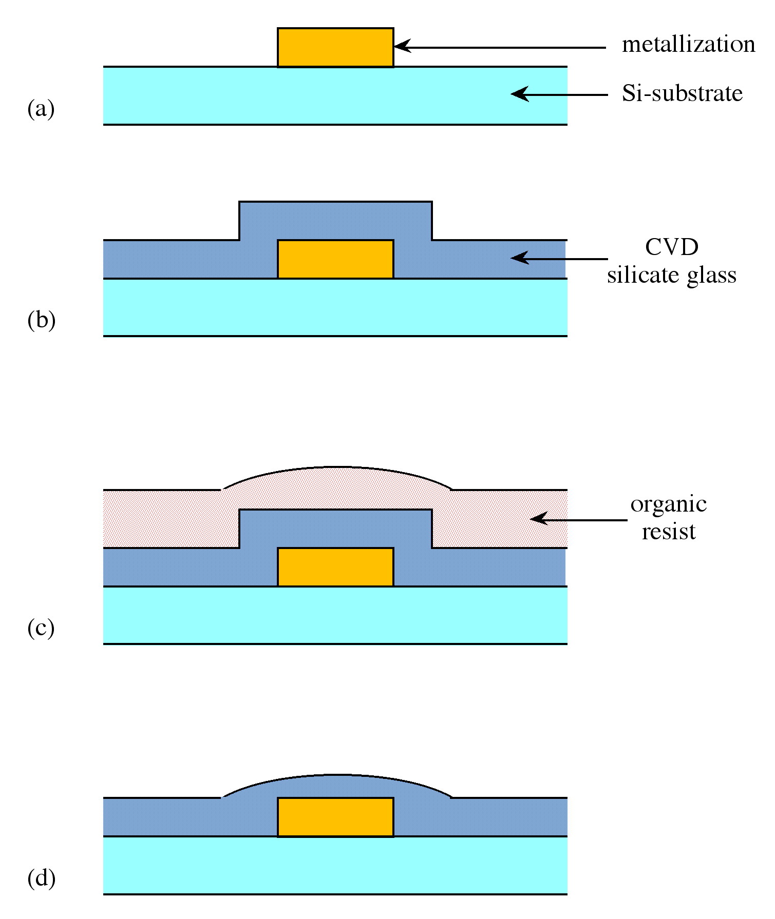
For the vast majority of electronic devices, the starting point is a substrate consisting of a flat single crystal wafer of semiconducting material. During processing, which includes the growth of both insulating and conducting films, the surface becomes increasingly non-planar. For example, a gate oxide in a typical MOSFET (see Figure \(\PageIndex{1}\)) may be typically 100 - 250 Å thick, while the isolation or field oxide may be 10,000 Å. In order for the successful subsequent deposition of conducting layers (metallization) to occur without breaking metal lines (often due to the difficulty in maintaining step coverage), the surface must be flat and smooth. This process is called planarization, and can be carried out by a technique known as sacrificial etchback. An abrupt step (Figure \(\PageIndex{2}\)a) is coated with a conformal layer of a low melting dielectric, e.g., borophosphorosilicate glass, BPSG (Figure \(\PageIndex{2}\)b), and subsequently a sacrificial organic resin (Figure \(\PageIndex{2}\)c). The sample is then plasma etched such that the resin and dielectric are removed at the same rate. Since the plasma etch follows the contour of the organic resin, a smooth surface is left behind (Figure \(\PageIndex{2}\)d). The planarization process thus reduces step height differentials significantly. In addition regions or valleys between individual metallization elements (vias) can be completely filled allowing for a route to producing uniformly flat surfaces, e.g., the BPSG film shown in Figure \(\PageIndex{1}\).

The processes of planarization is vital for the development of multilevel structures in VLSI circuits. To minimize interconnection resistance and conserve chip area, multilevel metallization schemes are being developed in which the interconnects run in 3-dimensions.
Bibliography
- J. L. Vossen and W. Kern, Phys. Today, 1980, 33, 26.
- S. K. Ghandhi, VLSI Fabrication Principles, Silicon and Gallium Arsenide, Wiley, Chichester, 2nd Ed. (1994).
- S. M. Sze, Physics of Semiconductor Devices, 2nd Edition, John Wiley & Sons, New York (1981).
- W. E. Beadle, J. C. C. Tsai, R. D. Plummer, Quick Reference Manual for Silicon Integrated Cuircuit Technology, Wiley, Chichester (1985).
- A. C. Adams and C. D. Capio, J. Electrochem. Soc., 1981, 128, 2630.

