
Covalent-Network Solids: Semiconductors and Insulators
- Page ID
- 53669
\( \newcommand{\vecs}[1]{\overset { \scriptstyle \rightharpoonup} {\mathbf{#1}} } \)
\( \newcommand{\vecd}[1]{\overset{-\!-\!\rightharpoonup}{\vphantom{a}\smash {#1}}} \)
\( \newcommand{\dsum}{\displaystyle\sum\limits} \)
\( \newcommand{\dint}{\displaystyle\int\limits} \)
\( \newcommand{\dlim}{\displaystyle\lim\limits} \)
\( \newcommand{\id}{\mathrm{id}}\) \( \newcommand{\Span}{\mathrm{span}}\)
( \newcommand{\kernel}{\mathrm{null}\,}\) \( \newcommand{\range}{\mathrm{range}\,}\)
\( \newcommand{\RealPart}{\mathrm{Re}}\) \( \newcommand{\ImaginaryPart}{\mathrm{Im}}\)
\( \newcommand{\Argument}{\mathrm{Arg}}\) \( \newcommand{\norm}[1]{\| #1 \|}\)
\( \newcommand{\inner}[2]{\langle #1, #2 \rangle}\)
\( \newcommand{\Span}{\mathrm{span}}\)
\( \newcommand{\id}{\mathrm{id}}\)
\( \newcommand{\Span}{\mathrm{span}}\)
\( \newcommand{\kernel}{\mathrm{null}\,}\)
\( \newcommand{\range}{\mathrm{range}\,}\)
\( \newcommand{\RealPart}{\mathrm{Re}}\)
\( \newcommand{\ImaginaryPart}{\mathrm{Im}}\)
\( \newcommand{\Argument}{\mathrm{Arg}}\)
\( \newcommand{\norm}[1]{\| #1 \|}\)
\( \newcommand{\inner}[2]{\langle #1, #2 \rangle}\)
\( \newcommand{\Span}{\mathrm{span}}\) \( \newcommand{\AA}{\unicode[.8,0]{x212B}}\)
\( \newcommand{\vectorA}[1]{\vec{#1}} % arrow\)
\( \newcommand{\vectorAt}[1]{\vec{\text{#1}}} % arrow\)
\( \newcommand{\vectorB}[1]{\overset { \scriptstyle \rightharpoonup} {\mathbf{#1}} } \)
\( \newcommand{\vectorC}[1]{\textbf{#1}} \)
\( \newcommand{\vectorD}[1]{\overrightarrow{#1}} \)
\( \newcommand{\vectorDt}[1]{\overrightarrow{\text{#1}}} \)
\( \newcommand{\vectE}[1]{\overset{-\!-\!\rightharpoonup}{\vphantom{a}\smash{\mathbf {#1}}}} \)
\( \newcommand{\vecs}[1]{\overset { \scriptstyle \rightharpoonup} {\mathbf{#1}} } \)
\(\newcommand{\longvect}{\overrightarrow}\)
\( \newcommand{\vecd}[1]{\overset{-\!-\!\rightharpoonup}{\vphantom{a}\smash {#1}}} \)
\(\newcommand{\avec}{\mathbf a}\) \(\newcommand{\bvec}{\mathbf b}\) \(\newcommand{\cvec}{\mathbf c}\) \(\newcommand{\dvec}{\mathbf d}\) \(\newcommand{\dtil}{\widetilde{\mathbf d}}\) \(\newcommand{\evec}{\mathbf e}\) \(\newcommand{\fvec}{\mathbf f}\) \(\newcommand{\nvec}{\mathbf n}\) \(\newcommand{\pvec}{\mathbf p}\) \(\newcommand{\qvec}{\mathbf q}\) \(\newcommand{\svec}{\mathbf s}\) \(\newcommand{\tvec}{\mathbf t}\) \(\newcommand{\uvec}{\mathbf u}\) \(\newcommand{\vvec}{\mathbf v}\) \(\newcommand{\wvec}{\mathbf w}\) \(\newcommand{\xvec}{\mathbf x}\) \(\newcommand{\yvec}{\mathbf y}\) \(\newcommand{\zvec}{\mathbf z}\) \(\newcommand{\rvec}{\mathbf r}\) \(\newcommand{\mvec}{\mathbf m}\) \(\newcommand{\zerovec}{\mathbf 0}\) \(\newcommand{\onevec}{\mathbf 1}\) \(\newcommand{\real}{\mathbb R}\) \(\newcommand{\twovec}[2]{\left[\begin{array}{r}#1 \\ #2 \end{array}\right]}\) \(\newcommand{\ctwovec}[2]{\left[\begin{array}{c}#1 \\ #2 \end{array}\right]}\) \(\newcommand{\threevec}[3]{\left[\begin{array}{r}#1 \\ #2 \\ #3 \end{array}\right]}\) \(\newcommand{\cthreevec}[3]{\left[\begin{array}{c}#1 \\ #2 \\ #3 \end{array}\right]}\) \(\newcommand{\fourvec}[4]{\left[\begin{array}{r}#1 \\ #2 \\ #3 \\ #4 \end{array}\right]}\) \(\newcommand{\cfourvec}[4]{\left[\begin{array}{c}#1 \\ #2 \\ #3 \\ #4 \end{array}\right]}\) \(\newcommand{\fivevec}[5]{\left[\begin{array}{r}#1 \\ #2 \\ #3 \\ #4 \\ #5 \\ \end{array}\right]}\) \(\newcommand{\cfivevec}[5]{\left[\begin{array}{c}#1 \\ #2 \\ #3 \\ #4 \\ #5 \\ \end{array}\right]}\) \(\newcommand{\mattwo}[4]{\left[\begin{array}{rr}#1 \amp #2 \\ #3 \amp #4 \\ \end{array}\right]}\) \(\newcommand{\laspan}[1]{\text{Span}\{#1\}}\) \(\newcommand{\bcal}{\cal B}\) \(\newcommand{\ccal}{\cal C}\) \(\newcommand{\scal}{\cal S}\) \(\newcommand{\wcal}{\cal W}\) \(\newcommand{\ecal}{\cal E}\) \(\newcommand{\coords}[2]{\left\{#1\right\}_{#2}}\) \(\newcommand{\gray}[1]{\color{gray}{#1}}\) \(\newcommand{\lgray}[1]{\color{lightgray}{#1}}\) \(\newcommand{\rank}{\operatorname{rank}}\) \(\newcommand{\row}{\text{Row}}\) \(\newcommand{\col}{\text{Col}}\) \(\renewcommand{\row}{\text{Row}}\) \(\newcommand{\nul}{\text{Nul}}\) \(\newcommand{\var}{\text{Var}}\) \(\newcommand{\corr}{\text{corr}}\) \(\newcommand{\len}[1]{\left|#1\right|}\) \(\newcommand{\bbar}{\overline{\bvec}}\) \(\newcommand{\bhat}{\widehat{\bvec}}\) \(\newcommand{\bperp}{\bvec^\perp}\) \(\newcommand{\xhat}{\widehat{\xvec}}\) \(\newcommand{\vhat}{\widehat{\vvec}}\) \(\newcommand{\uhat}{\widehat{\uvec}}\) \(\newcommand{\what}{\widehat{\wvec}}\) \(\newcommand{\Sighat}{\widehat{\Sigma}}\) \(\newcommand{\lt}{<}\) \(\newcommand{\gt}{>}\) \(\newcommand{\amp}{&}\) \(\definecolor{fillinmathshade}{gray}{0.9}\)Skills to Develop
- Explain the properties of some covalent-network solids
- Describe semiconductors and some of their properties
You can read a quick introduction to covalent-network solids in the intro page. The basic idea is that to make a network of covalent bonds, each atom (or many of the atoms) have to make 3 or 4 bonds to other atoms. This means that covalent-network solids usually include carbon, silicon, and their neighbors in the periodic table. Here, we'll focus on simple, orderly structures like diamond, graphite, and pure silicon. There are also covalent-network solid oxides, like the silicates, in which oxygen atoms connect 2 silicon atoms, and each silicon atom connects to 4 oxygens. Partially covalent oxides are what most rocks and ceramics are made of.
Graphite
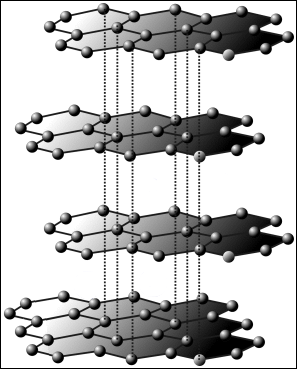
Carbon has 2 allotropes, or pure elemental forms. The more stable form is graphite, a dark, slippery material used in pencils and lubricants. Remember that carbon typically makes 4 bonds. The structure of graphite is flat hexagonal sheets; a single sheet is called graphene. Each carbon atom makes 3 σ bonds and the leftover p orbitals form a delocalized π-bond network over the whole sheet, very similar to the π-bonding in benzene. The π-bond system actually forms bands, like in a metal, allowing graphite to conduct electricity along the sheets. Weak interactions, like London dispersion forces, (called π-stacking in this case) hold the sheets loosely together. Because they can slide past each other (especially when impurity atoms are trapped in between) graphite is a good lubricant.
Diamond Structure
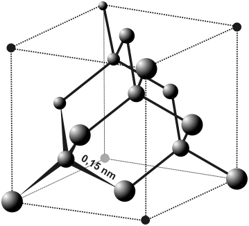
The other bulk allotrope of carbon is diamond. In diamond, each carbon makes 4 bonds in tetrahedral directions to other carbon atoms. The structure is like the zinc blende ionic structure, except that all the atoms are the same. The properties of diamond (insulator, hard) come from the strong covalent bonds. Remember that C-C bonds are some of the strongest covalent bonds. It's easiest to think about diamond as forming with sp3 hybrid orbitals on each atom. It's hard to imagine the MO interactions, but the main thing we can know is that because there is good energy match and good overlap between the atoms, the splitting (energy difference) between bonding and anti-bonding MOs will be big (and there won't be any non-bonding MOs, because each atom has 4 orbitals and makes 4 bonds). There will still be bands like in metals, but now there are 2 bands with a big energy gap in the middle. The low-energy, bonding band is called the valence band, and there are exactly enough electrons to fill it. The high-energy, anti-bonding band is called the conduction band, and it is empty.
If it was hard to understand the previous paragraph, let's just imagine making 1 bond between 2 atoms. We use one sp3 hybrid on each atom. These point right at each other, have exactly the same energy, and have good overlap. We can imagine drawing an MO diagram just like for H2, with a big energy gap between the bonding and anti-bonding orbitals. Each atom has 4 electrons total, and makes 4 bonds just like this, so each bond gets 1 electron from each atom: just enough to fill up the bonding MO. When we multiply this over all the bonds in the diamond, we get the full valence band and the empty conduction band. The energy gap between them is called the band gap. In diamond, the band gap is big, and so diamond is an insulator.
Semiconductors
Silicon has a structure just like diamond. (It doesn't make graphite, because mostly π-bonds are weak for the second-row elements.) However, silicon has a smaller band gap than diamond. Germanium, which is below silicon in the periodic table, has the same structure, and an even lower band gap. Generally, as we go down the periodic table, covalent bond strengths get smaller, which is the same as saying that the splitting between bonding and antibonding orbitals gets smaller. It's hard to say why, but if you assume that heavier atoms have worse orbital overlap, you will usually make good predictions.
Semiconductors are materials that conduct electricity just a little bit. They are the basis for all computing and electronics. Semiconductivity comes from having a not-quite-full valence band, a not-quite-empty conduction band, or both. If there are a few electrons in the conduction band, they can conduct electricity just like in a metal (except less, because there aren't very many of them!). If there are a few electrons missing from the valence band, the empty spots are called holes and they can move around, also conducting electricity. If the band gap of a material is not too big compared to the thermal energy, then a few electrons can be in the conduction band even though there is room for them in the valence band (because of thermal energy). For this reason, semiconductors conduct better at higher temperature, because more electrons will be in the conduction band.

Doping Semiconductors
The other way to make a semiconductor, with a material whose band gap is too big at room temperature, is by adding some impurity atoms with different numbers of electrons, which is called doping. Imagine that you have silicon with just a few nitrogen atoms replacing silicon atoms. Each N has an extra electron. Now there will be a few electrons in the conduction band, so it's a semiconductor! And we can control the conductivity by controlling how much N we add. We can do the same thing if we add a little bit of boron, which has 3 electrons. In this case, there would be a few holes in the valence band. These are called p-type (positive, less electrons, like with B) or n-type (negative, extra electrons, like with N) semiconductors. Lots of important devices, like LEDs, solar cells and transistors (the basis of computer chips) are made of layers of p-type and n-type semiconductors.
Compound Semiconductors
We can also make semiconductors that are compounds, like gallium arsenide (formula GaAs). These have an AB formula, and there are always 8 valence electrons in the formula. For example, Ga has 3 and As has 5, so GaAs has 8. Another example is ZnSe, (Zn has 2 valence electrons in 4s, Se has 6 valence electrons just like O). Thus, they have the same number of valence electrons as C or Si. They also have the same structure (zinc blende, just like diamond except that that atoms alternate types). By combining many different elements, we can change various properties, like band gap, to be exactly what we want. Generally, the band gap increases as the 2 elements are farther apart (the bonding becomes more ionic, and ionic solids aren't conductive). We can even mix 3 or more elements, like in CdZnTe (the actual formula would probably be written (Cd,Zn)Te, meaning that the number of Cd + Zn = Te). To make semiconductors with the right properties, we can use different combinations of elements and also dope with many different elements.
Contributors and Attributions
Emily V Eames (City College of San Francisco)