9.11: Bonding in Semiconductors
- Page ID
- 84729
\( \newcommand{\vecs}[1]{\overset { \scriptstyle \rightharpoonup} {\mathbf{#1}} } \)
\( \newcommand{\vecd}[1]{\overset{-\!-\!\rightharpoonup}{\vphantom{a}\smash {#1}}} \)
\( \newcommand{\id}{\mathrm{id}}\) \( \newcommand{\Span}{\mathrm{span}}\)
( \newcommand{\kernel}{\mathrm{null}\,}\) \( \newcommand{\range}{\mathrm{range}\,}\)
\( \newcommand{\RealPart}{\mathrm{Re}}\) \( \newcommand{\ImaginaryPart}{\mathrm{Im}}\)
\( \newcommand{\Argument}{\mathrm{Arg}}\) \( \newcommand{\norm}[1]{\| #1 \|}\)
\( \newcommand{\inner}[2]{\langle #1, #2 \rangle}\)
\( \newcommand{\Span}{\mathrm{span}}\)
\( \newcommand{\id}{\mathrm{id}}\)
\( \newcommand{\Span}{\mathrm{span}}\)
\( \newcommand{\kernel}{\mathrm{null}\,}\)
\( \newcommand{\range}{\mathrm{range}\,}\)
\( \newcommand{\RealPart}{\mathrm{Re}}\)
\( \newcommand{\ImaginaryPart}{\mathrm{Im}}\)
\( \newcommand{\Argument}{\mathrm{Arg}}\)
\( \newcommand{\norm}[1]{\| #1 \|}\)
\( \newcommand{\inner}[2]{\langle #1, #2 \rangle}\)
\( \newcommand{\Span}{\mathrm{span}}\) \( \newcommand{\AA}{\unicode[.8,0]{x212B}}\)
\( \newcommand{\vectorA}[1]{\vec{#1}} % arrow\)
\( \newcommand{\vectorAt}[1]{\vec{\text{#1}}} % arrow\)
\( \newcommand{\vectorB}[1]{\overset { \scriptstyle \rightharpoonup} {\mathbf{#1}} } \)
\( \newcommand{\vectorC}[1]{\textbf{#1}} \)
\( \newcommand{\vectorD}[1]{\overrightarrow{#1}} \)
\( \newcommand{\vectorDt}[1]{\overrightarrow{\text{#1}}} \)
\( \newcommand{\vectE}[1]{\overset{-\!-\!\rightharpoonup}{\vphantom{a}\smash{\mathbf {#1}}}} \)
\( \newcommand{\vecs}[1]{\overset { \scriptstyle \rightharpoonup} {\mathbf{#1}} } \)
\( \newcommand{\vecd}[1]{\overset{-\!-\!\rightharpoonup}{\vphantom{a}\smash {#1}}} \)
\(\newcommand{\avec}{\mathbf a}\) \(\newcommand{\bvec}{\mathbf b}\) \(\newcommand{\cvec}{\mathbf c}\) \(\newcommand{\dvec}{\mathbf d}\) \(\newcommand{\dtil}{\widetilde{\mathbf d}}\) \(\newcommand{\evec}{\mathbf e}\) \(\newcommand{\fvec}{\mathbf f}\) \(\newcommand{\nvec}{\mathbf n}\) \(\newcommand{\pvec}{\mathbf p}\) \(\newcommand{\qvec}{\mathbf q}\) \(\newcommand{\svec}{\mathbf s}\) \(\newcommand{\tvec}{\mathbf t}\) \(\newcommand{\uvec}{\mathbf u}\) \(\newcommand{\vvec}{\mathbf v}\) \(\newcommand{\wvec}{\mathbf w}\) \(\newcommand{\xvec}{\mathbf x}\) \(\newcommand{\yvec}{\mathbf y}\) \(\newcommand{\zvec}{\mathbf z}\) \(\newcommand{\rvec}{\mathbf r}\) \(\newcommand{\mvec}{\mathbf m}\) \(\newcommand{\zerovec}{\mathbf 0}\) \(\newcommand{\onevec}{\mathbf 1}\) \(\newcommand{\real}{\mathbb R}\) \(\newcommand{\twovec}[2]{\left[\begin{array}{r}#1 \\ #2 \end{array}\right]}\) \(\newcommand{\ctwovec}[2]{\left[\begin{array}{c}#1 \\ #2 \end{array}\right]}\) \(\newcommand{\threevec}[3]{\left[\begin{array}{r}#1 \\ #2 \\ #3 \end{array}\right]}\) \(\newcommand{\cthreevec}[3]{\left[\begin{array}{c}#1 \\ #2 \\ #3 \end{array}\right]}\) \(\newcommand{\fourvec}[4]{\left[\begin{array}{r}#1 \\ #2 \\ #3 \\ #4 \end{array}\right]}\) \(\newcommand{\cfourvec}[4]{\left[\begin{array}{c}#1 \\ #2 \\ #3 \\ #4 \end{array}\right]}\) \(\newcommand{\fivevec}[5]{\left[\begin{array}{r}#1 \\ #2 \\ #3 \\ #4 \\ #5 \\ \end{array}\right]}\) \(\newcommand{\cfivevec}[5]{\left[\begin{array}{c}#1 \\ #2 \\ #3 \\ #4 \\ #5 \\ \end{array}\right]}\) \(\newcommand{\mattwo}[4]{\left[\begin{array}{rr}#1 \amp #2 \\ #3 \amp #4 \\ \end{array}\right]}\) \(\newcommand{\laspan}[1]{\text{Span}\{#1\}}\) \(\newcommand{\bcal}{\cal B}\) \(\newcommand{\ccal}{\cal C}\) \(\newcommand{\scal}{\cal S}\) \(\newcommand{\wcal}{\cal W}\) \(\newcommand{\ecal}{\cal E}\) \(\newcommand{\coords}[2]{\left\{#1\right\}_{#2}}\) \(\newcommand{\gray}[1]{\color{gray}{#1}}\) \(\newcommand{\lgray}[1]{\color{lightgray}{#1}}\) \(\newcommand{\rank}{\operatorname{rank}}\) \(\newcommand{\row}{\text{Row}}\) \(\newcommand{\col}{\text{Col}}\) \(\renewcommand{\row}{\text{Row}}\) \(\newcommand{\nul}{\text{Nul}}\) \(\newcommand{\var}{\text{Var}}\) \(\newcommand{\corr}{\text{corr}}\) \(\newcommand{\len}[1]{\left|#1\right|}\) \(\newcommand{\bbar}{\overline{\bvec}}\) \(\newcommand{\bhat}{\widehat{\bvec}}\) \(\newcommand{\bperp}{\bvec^\perp}\) \(\newcommand{\xhat}{\widehat{\xvec}}\) \(\newcommand{\vhat}{\widehat{\vvec}}\) \(\newcommand{\uhat}{\widehat{\uvec}}\) \(\newcommand{\what}{\widehat{\wvec}}\) \(\newcommand{\Sighat}{\widehat{\Sigma}}\) \(\newcommand{\lt}{<}\) \(\newcommand{\gt}{>}\) \(\newcommand{\amp}{&}\) \(\definecolor{fillinmathshade}{gray}{0.9}\)- With the aid of simple diagrams, show how different band energy ranges in solids can produce conductors, insulators, and semiconductors.
- Describe the nature and behavior of a simple PN junction.
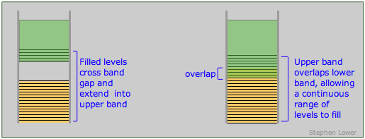
The band theory of solids provides a clear set of criteria for distinguishing between conductors (metals), insulators and semiconductors. As we have seen, a conductor must posses an upper range of allowed levels that are only partially filled with valence electrons. These levels can be within a single band, or they can be the combination of two overlapping bands. A band structure of this type is known as a conduction band.

Band arrangements in conductors. Metallic conduction requires the presence of empty levels into which electrons can move as they acquire momentum. This can be achieved when a band is only partially occupied or overlaps an empty band (right), or when the gap between a filled band and an upper empty one is sufficiently small (left) to allow ordinary thermal energy to supply the promotion energy.
Insulators and semiconductors
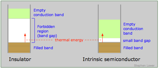
An insulator is characterized by a large band gap between the highest filled band and an even higher empty band. The band gap is sufficiently great to prevent any significant population of the upper band by thermal excitation of electrons from the lower one. The presence of a very intense electric field may be able to supply the required energy, in which case the insulator undergoes dielectric breakdown. Most molecular crystals are insulators, as are covalent crystals such as diamond.

If the band gap is sufficiently small to allow electrons in the filled band below it to jump into the upper empty band by thermal excitation, the solid is known as a semiconductor. In contrast to metals, whose electrical conductivity decreases with temperature (the more intense lattice vibrations interfere with the transfer of momentum by the electron fluid), the conductivity of semiconductors increases with temperature. In many cases the excitation energy can be provided by absorption of light, so most semiconductors are also photoconductors. Examples of semiconducting elements are Se, Te, Bi, Ge, Si, and graphite.
The presence of an impurity in a semiconductor can introduce a new band into the system. If this new band is situated within the forbidden region, it creates a new and smaller band gap that will increase the conductivity. The huge semiconductor industry is based on the ability to tailor the band gap to fit the desired application by introducing an appropriate impurity atom (dopant) into the semiconductor lattice. The dopant elements are normally atoms whose valance shells contain one electron more or less than the atoms of the host crystal.
Semiconductor materials have traditionally been totally inorganic, composed mostly of the lighter P-block elements. More recently, organic semiconductors have become an important field of study and development.
Thermal properties of Semiconductors
At absolute zero, all of the charge carriers reside in lower of the bands below the small band gap in a semiconductor (that is, in the valence band of the illustration on the left above, or in the impurity band of the one on the right.) At higher temperatures, thermal excitation of the electrons allows an increasing fraction jump across this band gap and populate either the empty impurity band or the conduction band as shown at the right. The effect is the same in either case; the semiconductor becomes more conductive as the temperature is raised. Note that this is just the opposite to the way temperature affects the conductivity of metals.

N- and P-type materials

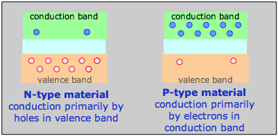
For example, a phosphorus atom introduced as an impurity into a silicon lattice possesses one more valence electron than Si. This electron is delocalized within the impurity band and serves as the charge carrier in what is known as an N-type semiconductor. In a semiconductor of the P-type, the dopant might be arsenic, which has only three valence electrons. This creates what amounts to an electron deficiency or hole in the electron fabric of the crystal, although the solid remains electrically neutral overall. As this vacancy is filled by the electrons from silicon atoms the vacancy hops to another location, so the charge carrier is effectively a positively charged hole, hence the P-type designation.

Substitution of just one dopant atom into 107 atoms of Si can increase the conductivity by a factor of 100,000.
The PN junction
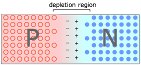
When P- and N-type materials are brought into contact, creating a PN junction. Holes in the P material and electrons in the N material drift toward and neutralize each other, creating a depletion region that is devoid of charge carriers. But the destruction of these carriers leaves immobile positive ions in the N material and negative ions in the P material, giving rise to an interfacial potential difference ("space charge") as depicted here.

As this charge builds up, it acts to resist the further diffusion of electrons and holes, leaving a carrier-free depletion region, which acts as a barrier at the junction interface.


