
6.12: Electronic Grade Gallium Arsenide
- Page ID
- 212888
\( \newcommand{\vecs}[1]{\overset { \scriptstyle \rightharpoonup} {\mathbf{#1}} } \)
\( \newcommand{\vecd}[1]{\overset{-\!-\!\rightharpoonup}{\vphantom{a}\smash {#1}}} \)
\( \newcommand{\id}{\mathrm{id}}\) \( \newcommand{\Span}{\mathrm{span}}\)
( \newcommand{\kernel}{\mathrm{null}\,}\) \( \newcommand{\range}{\mathrm{range}\,}\)
\( \newcommand{\RealPart}{\mathrm{Re}}\) \( \newcommand{\ImaginaryPart}{\mathrm{Im}}\)
\( \newcommand{\Argument}{\mathrm{Arg}}\) \( \newcommand{\norm}[1]{\| #1 \|}\)
\( \newcommand{\inner}[2]{\langle #1, #2 \rangle}\)
\( \newcommand{\Span}{\mathrm{span}}\)
\( \newcommand{\id}{\mathrm{id}}\)
\( \newcommand{\Span}{\mathrm{span}}\)
\( \newcommand{\kernel}{\mathrm{null}\,}\)
\( \newcommand{\range}{\mathrm{range}\,}\)
\( \newcommand{\RealPart}{\mathrm{Re}}\)
\( \newcommand{\ImaginaryPart}{\mathrm{Im}}\)
\( \newcommand{\Argument}{\mathrm{Arg}}\)
\( \newcommand{\norm}[1]{\| #1 \|}\)
\( \newcommand{\inner}[2]{\langle #1, #2 \rangle}\)
\( \newcommand{\Span}{\mathrm{span}}\) \( \newcommand{\AA}{\unicode[.8,0]{x212B}}\)
\( \newcommand{\vectorA}[1]{\vec{#1}} % arrow\)
\( \newcommand{\vectorAt}[1]{\vec{\text{#1}}} % arrow\)
\( \newcommand{\vectorB}[1]{\overset { \scriptstyle \rightharpoonup} {\mathbf{#1}} } \)
\( \newcommand{\vectorC}[1]{\textbf{#1}} \)
\( \newcommand{\vectorD}[1]{\overrightarrow{#1}} \)
\( \newcommand{\vectorDt}[1]{\overrightarrow{\text{#1}}} \)
\( \newcommand{\vectE}[1]{\overset{-\!-\!\rightharpoonup}{\vphantom{a}\smash{\mathbf {#1}}}} \)
\( \newcommand{\vecs}[1]{\overset { \scriptstyle \rightharpoonup} {\mathbf{#1}} } \)
\( \newcommand{\vecd}[1]{\overset{-\!-\!\rightharpoonup}{\vphantom{a}\smash {#1}}} \)
\(\newcommand{\avec}{\mathbf a}\) \(\newcommand{\bvec}{\mathbf b}\) \(\newcommand{\cvec}{\mathbf c}\) \(\newcommand{\dvec}{\mathbf d}\) \(\newcommand{\dtil}{\widetilde{\mathbf d}}\) \(\newcommand{\evec}{\mathbf e}\) \(\newcommand{\fvec}{\mathbf f}\) \(\newcommand{\nvec}{\mathbf n}\) \(\newcommand{\pvec}{\mathbf p}\) \(\newcommand{\qvec}{\mathbf q}\) \(\newcommand{\svec}{\mathbf s}\) \(\newcommand{\tvec}{\mathbf t}\) \(\newcommand{\uvec}{\mathbf u}\) \(\newcommand{\vvec}{\mathbf v}\) \(\newcommand{\wvec}{\mathbf w}\) \(\newcommand{\xvec}{\mathbf x}\) \(\newcommand{\yvec}{\mathbf y}\) \(\newcommand{\zvec}{\mathbf z}\) \(\newcommand{\rvec}{\mathbf r}\) \(\newcommand{\mvec}{\mathbf m}\) \(\newcommand{\zerovec}{\mathbf 0}\) \(\newcommand{\onevec}{\mathbf 1}\) \(\newcommand{\real}{\mathbb R}\) \(\newcommand{\twovec}[2]{\left[\begin{array}{r}#1 \\ #2 \end{array}\right]}\) \(\newcommand{\ctwovec}[2]{\left[\begin{array}{c}#1 \\ #2 \end{array}\right]}\) \(\newcommand{\threevec}[3]{\left[\begin{array}{r}#1 \\ #2 \\ #3 \end{array}\right]}\) \(\newcommand{\cthreevec}[3]{\left[\begin{array}{c}#1 \\ #2 \\ #3 \end{array}\right]}\) \(\newcommand{\fourvec}[4]{\left[\begin{array}{r}#1 \\ #2 \\ #3 \\ #4 \end{array}\right]}\) \(\newcommand{\cfourvec}[4]{\left[\begin{array}{c}#1 \\ #2 \\ #3 \\ #4 \end{array}\right]}\) \(\newcommand{\fivevec}[5]{\left[\begin{array}{r}#1 \\ #2 \\ #3 \\ #4 \\ #5 \\ \end{array}\right]}\) \(\newcommand{\cfivevec}[5]{\left[\begin{array}{c}#1 \\ #2 \\ #3 \\ #4 \\ #5 \\ \end{array}\right]}\) \(\newcommand{\mattwo}[4]{\left[\begin{array}{rr}#1 \amp #2 \\ #3 \amp #4 \\ \end{array}\right]}\) \(\newcommand{\laspan}[1]{\text{Span}\{#1\}}\) \(\newcommand{\bcal}{\cal B}\) \(\newcommand{\ccal}{\cal C}\) \(\newcommand{\scal}{\cal S}\) \(\newcommand{\wcal}{\cal W}\) \(\newcommand{\ecal}{\cal E}\) \(\newcommand{\coords}[2]{\left\{#1\right\}_{#2}}\) \(\newcommand{\gray}[1]{\color{gray}{#1}}\) \(\newcommand{\lgray}[1]{\color{lightgray}{#1}}\) \(\newcommand{\rank}{\operatorname{rank}}\) \(\newcommand{\row}{\text{Row}}\) \(\newcommand{\col}{\text{Col}}\) \(\renewcommand{\row}{\text{Row}}\) \(\newcommand{\nul}{\text{Nul}}\) \(\newcommand{\var}{\text{Var}}\) \(\newcommand{\corr}{\text{corr}}\) \(\newcommand{\len}[1]{\left|#1\right|}\) \(\newcommand{\bbar}{\overline{\bvec}}\) \(\newcommand{\bhat}{\widehat{\bvec}}\) \(\newcommand{\bperp}{\bvec^\perp}\) \(\newcommand{\xhat}{\widehat{\xvec}}\) \(\newcommand{\vhat}{\widehat{\vvec}}\) \(\newcommand{\uhat}{\widehat{\uvec}}\) \(\newcommand{\what}{\widehat{\wvec}}\) \(\newcommand{\Sighat}{\widehat{\Sigma}}\) \(\newcommand{\lt}{<}\) \(\newcommand{\gt}{>}\) \(\newcommand{\amp}{&}\) \(\definecolor{fillinmathshade}{gray}{0.9}\)Introduction
The synthesis and purification of bulk polycrystalline semiconductor material represents the first step towards the commercial fabrication of an electronic device. This polycrystalline material is then used as the raw material for the formation of single crystal material that is processed to semiconductor wafers.
In contrast to electronic grade silicon (EGS), whose use is a minor fraction of the global production of elemental silicon, gallium arsenide (GaAs) is produced exclusively for use in the semiconductor industry. However, arsenic and its compounds have significant commercial applications. The main use of elemental arsenic is in alloys of Pb, and to a lesser extent Cu, while arsenic compounds are widely used in pesticides and wood preservatives and the production of bottle glass. Thus, the electronics industry represents a minor user of arsenic. In contrast, although gallium has minor uses as a high-temperature liquid seal, manometric fluids and heat transfer media, and for low temperature solders, its main use is in semiconductor technology.
Isolation and purification of gallium metal
At 19 ppm gallium (L. Gallia, France) is about as abundant as nitrogen, lithium and lead; it is twice as abundant as boron (9 ppm), but is more difficult to extract due to the lack of any major gallium-containing ore. Gallium always occurs in association either with zinc or germanium, its neighbors in the periodic table, or with aluminum in the same group. Thus, the highest concentrations (0.1-1%) are in the rare mineral germanite (a complex sulfide of Zn, Cu, Ge, and As), while concentrations in sphalerite (ZnS), diaspore [AlO(OH)], bauxite, or coal, are a hundred-fold less. Industrially, gallium was originally recovered from the flue dust emitted during sulfide roasting or coal burning (up to 1.5% Ga), however, it is now obtained as side product of vast aluminum industry and in particular from the Bayer process for obtaining alumina from bauxite.
The Bayer process involves dissolution of bauxite, AlOxOH3-2x, in aqueous NaOH, separation of insoluble impurities, partial precipitation of the trihydrate, Al(OH)3, and calcination at 1,200 °C. During processing the alkaline solution is gradually enriched in gallium from an initial weight ratio Ga/Al of about 1/5000 to about 1/300. Electrolysis of these extracts with a Hg cathode results in further concentration, and the solution of sodium gallate thus formed is then electrolyzed with a stainless steel cathode to give Ga metal. Since bauxite contains 0.003-0.01% gallium, complete recovery would yield some 500-1000 tons per annum, however present consumption is only 0.1% of this about 10 tons per annum.
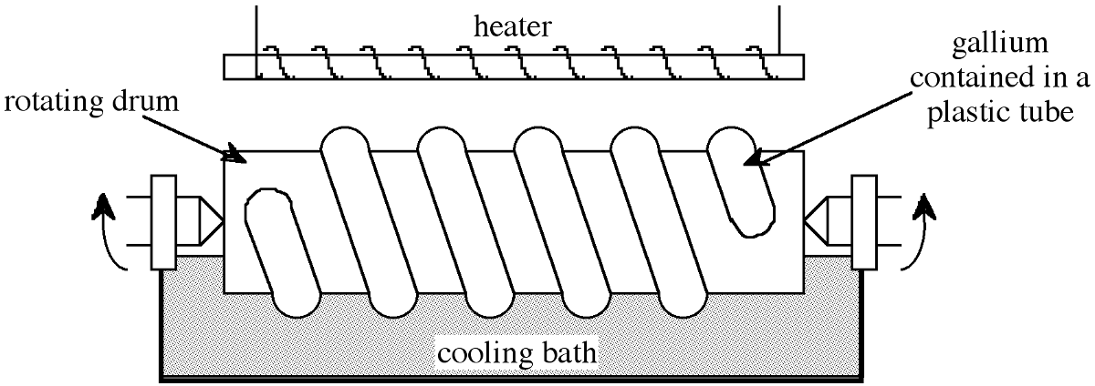
A typical analysis of the 98-99% pure gallium obtained as a side product from the Bayer process is shown in Table \(\PageIndex{1}\). This material is further purified to 99.99% by chemical treatment with acids and O2 at high temperatures followed by crystallization. This chemical process results in the reduction of the majority of metal impurities at the ppm level, see Table \(\PageIndex{1}\). Purification to seven nines 99.9999% is possible through zone refining, however, since the equilibrium distribution coefficient of the residual impurities k0 ≈ 1, multiple passes are required, typically > 500. The low melting point of gallium ensures that contamination from the container wall (which is significant in silicon zone refining) is minimized. In order to facilitate the multiple zone refining in a suitable time, a simple modification of zone refining is employed shown in Figure \(\PageIndex{1}\). The gallium is contained in a plastic tube wrapped around a rotating cylinder that is half immersed in a cooling bath. A heater is positioned above the gallium plastic coil. Thus, establishing a series of molten zones that pass upon rotation of the drum by one helical segment per revolution. In this manner, 500 passes may be made in relatively short time periods. The typical impurity levels of gallium zone refined in this manner are given in Table \(\PageIndex{1}\).
| Element | Bayer process (ppm) | After acid/base leaching (ppm) | 500 zone passes (ppm) |
|---|---|---|---|
| aluminum | 100-1,000 | 7 | < 1 |
| calcium | 10-100 | not detected | not detected |
| copper | 100-1,000 | 2 | < 1 |
| iron | 100-1,000 | 7 | < 1 |
| lead | < 2000 | 30 | not detected |
| magnesium | 10-100 | 1 | not detected |
| mercury | 10-100 | not detected | not detected |
| nickel | 10-100 | not detected | not detected |
| silicon | 10-100 | ≈ 1 | not detected |
| tin | 10-100 | ≈ 1 | not detected |
| titanium | 10-100 | 1 | < 1 |
| zinc | 30,000 | ≈ 1 | not detected |
Isolation and purification of elemental arsenic
Elemental arsenic (L. arsenicum, yellow orpiment) exists in two forms: yellow (cubic, As4) and gray or metallic (rhombohedral). At a natural abundance of 1.8 ppm arsenic is relatively rare, however, this is offset by its presence in a number of common minerals and the relative ease of isolation. Arsenic containing minerals are grouped into three main classes: the sulfides realgar (As4S4) and orpiment (As2S3), the oxide arsenolite (As2O3), and the arsenides and sulfaresenides of the iron, cobalt, and nickel. Minerals in this latter class include: loellinginite (FeAs2), safforlite (CoAs), niccolite (NiAs), rammelsbergite (NiAs2), ansenopyrite or mispickel (FeAsS), cobaltite (CoAsS), enargite (Cu3AsS4), gerdsorfite (NiAsS), and the quarturnary sulfide glaucodot [(Co,Fe)AsS]. Table \(\PageIndex{2}\) shows the typical impurities in arsenopyrite.
| Element | Concentration (ppm) | Element | Concentration (ppm) |
|---|---|---|---|
| silver | 90 | nickel | < 3,000 |
| gold | 8 | lead | 50 |
| cobalt | 30,000 | platinum | 0.4 |
| copper | 200 | rhenium | 50 |
| germanium | 30 | selenium | 50 |
| manganese | 3,000 | vanadium | 300 |
| molybdenum | 60 | zinc | 400 |
Arsenic is obtained commercially by smelting either FeAs2 or FeAsS at 650-700 °C in the absence of air and condensing the sublimed element (Tsub = 613 °C), (6.12.1).
\[ \text{FeAsS} \xrightarrow{\text{650-700 °C}} \text{FeS + As(vapor)} \xrightarrow{\text{<613 °C}} \text{As(solid)}\]
The arsenic thus obtained is combined with lead and then sublimed (Tsub = 614 °C) which binds any sulfur impurities more strongly than arsenic. Any residual arsenic that remains trapped in the iron sulfide is separated by forming the oxide (As2O3) by roasting the sulfide in air. The oxide is sublimed into the flue system during roasting from where it is collected and reduced with charcoal at 700-800 °C to give elemental arsenic. Semiconductor grade arsenic (> 99.9999%) is formed by zone refining.
Synthesis and purification of gallium arsenide.
Gallium arsenide can be prepared by the direct reaction of the elements, (6.12.2). However, while conceptually simple the synthesis of GaAs is complicated by the different vapor pressures of the reagents and the highly exothermic nature of the reaction. Furthermore, since the synthesis of GaAs at atmospheric pressure is accompanied by its simultaneous decomposes due to the loss by sublimation, of arsenic, the synthesis must be carried out under an overpressure of arsenic in order to maintain a stoichiometric composition of the synthesized GaAs.
\[ \text{Ga(liquid) + As(vapor)} \xrightarrow{ \text{>1240 °C}} \text{GaAs(solid)}\]
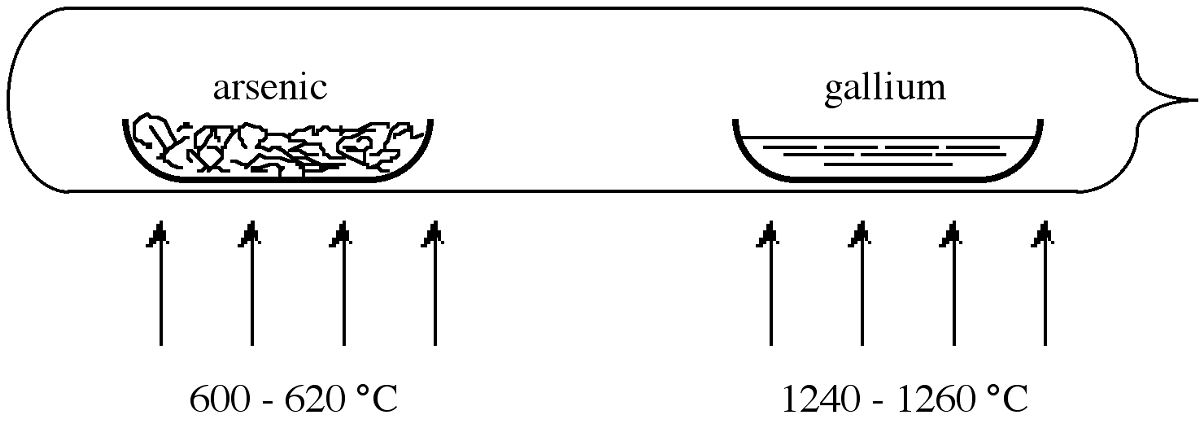
In order to overcome the problems associated with arsenic loss, the reaction is usually carried out in a sealed reaction tube. However, if a stoichiometric quantity of arsenic is used in the reaction a constant temperature of 1238 °C must be employed in order to maintain the desired arsenic overpressure of 1 atm. Practically, it is easier to use a large excess of arsenic heated to a lower temperature. In this situation the pressure in the tube is approximately equal to the equilibrium vapor pressure of the volatile component (arsenic) at the lower temperature. Thus, an over pressure of 1 atm arsenic may be maintained if within a sealed tube elemental arsenic is heated to 600-620 °C while the GaAs is maintained at 1240-1250 °C.
Figure \(\PageIndex{2}\) shows the sealed tube configuration that is typically used for the synthesis of GaAs. The tube is heated within a two-zone furnace. The boats holding the reactants are usually made of quartz, however, graphite is also used since the latter has a closer thermal expansion match to the GaAs product. If higher purity is required then pyrolytic boron nitride (PBN) is used. One of the boats is loaded with pure gallium the other with arsenic. A plug of quartz wool may be placed between the boats to act as a diffuser. The tube is then evacuated and sealed. Once brought to the correct reaction temperatures (Figure \(\PageIndex{2}\)), the arsenic vapor is transported to the gallium, and they react to form GaAs in a controlled manner. Table \(\PageIndex{3}\) gives the typical impurity concentrations found in polycrystalline GaAs.
| Element | Concentration (ppm) | Element | Concentration (ppm) |
|---|---|---|---|
| boron | 0.1 | silicon | 0.02 |
| carbon | 0.7 | phosphorus | 0.1 |
| nitrogen | 0.1 | sulfur | 0.01 |
| oxygen | 0.5 | chlorine | 0.08 |
| fluorine | 0.2 | nickel | 0.04 |
| magnesium | 0.02 | copper | 0.01 |
| aluminum | 0.02 | zinc | 0.05 |
Polycrystalline GaAs, formed in from the direct reaction of the elements is often used as the starting material for single crystal growth via Bridgeman or Czochralski crystal growth. It is also possible to prepare single crystals of GaAs directly from the elements using in-situ, or direct, compounding within a high-pressure liquid encapsulated Czochralski (HPLEC) technique.
Growth of gallium arsenide crystals
When considering the synthesis of Group 13-15 compounds for electronic applications, the very nature of semiconductor behavior demands the use of high purity single crystal materials. The polycrystalline materials synthesized above are, therefore, of little use for 13-15 semiconductors but may, however, serve as the starting material for melt grown single crystals. For GaAs, undoubtedly the most important 13-15 (III - V) semiconductor, melt grown single crystals are achieved by one of two techniques: the Bridgman technique, and the Czochralski technique.
Bridgman growth
The Bridgman technique requires a two-zone furnace, of the type shown in Figure \(\PageIndex{3}\). The left hand zone is maintained at a temperature of ca. 610 °C, allowing sufficient overpressure of arsenic within the sealed system to prevent arsenic loss from the gallium arsenide. The right hand side of the furnace contains the polycrystalline GaAs raw material held at a temperature just above its melting point (ca. 1240 °C). As the furnace moves from left to right, the melt cools and solidifies.
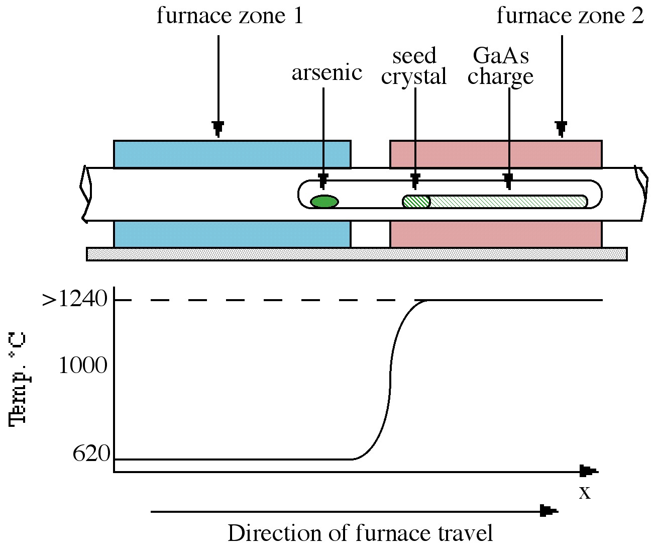
If a seed crystal is placed at the left hand side of the melt (at a point where the temperature gradient is such that only the end melts), a specific orientation of single crystal may be propagated at the liquid-solid interface eventually to produce a single crystal.
Czochralski growth
The Czochralski technique, which is the most commonly used technique in industry, is shown in Figure \(\PageIndex{4}\). The process relies on the controlled withdrawal of a seed crystal from a liquid melt. As the seed is lowered into the melt, partial melting of the tip occurs creating the liquid solid interface required for crystal growth. As the seed is withdrawn, solidification occurs and the seed orientation is propagated into the grown material. The variable parameters of rate of withdrawal and rotation rate can control crystal diameter and purity. As shown in Figure \(\PageIndex{4}\) the GaAs melt is capped by boron trioxide (B2O3). The capping layer, which is inert to GaAs, prevents arsenic loss when the pressure on the surface is above atmospheric pressure. The growth of GaAs by this technique is thus termed liquid encapsulated Czochralski (LEC) growth.
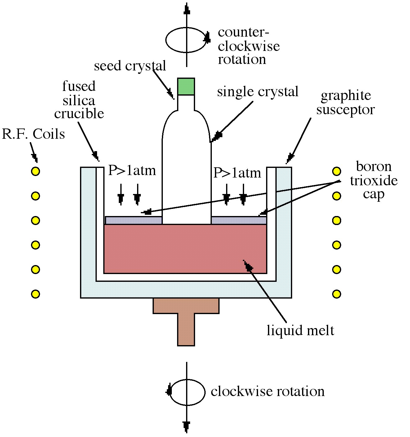
While the Bridgman technique is largely favored for GaAs growth, larger diameter wafers can be obtained by the Czochralski method. Both of these melt techniques produce materials heavily contaminated by the crucible, making them suitable almost exclusively as substrate material. Another disadvantage of these techniques is the production of defects in the material caused by the melt process.
Bibliography
- S. K. Ghandhi, VLSI Fabrication Principles: Silicon and Gallium Arsenide. Wiley-Interscience, New York, (1994).
- J. Krauskopf, J. D. Meyer, B. Wiedemann, M. Waldschmidt, K. Bethge, G. Wolf, and W. Schültze, 5th Conference on Semi-insulating III-V Materials, Malmo, Sweden, 1988, Eds. G. Grossman and L. Ledebo, Adam-Hilger, New York (1988).
- W. G. Pfann, Zone Melting, John Wiley & Sons, New York (1966).
- R. E. Williams, Gallium Arsenide Processing Techniques. Artech House (1984).
- Properties of Gallium Arsenide. Ed. M. R. Brozel and G. E. Stillman. 3rd Ed. Institution of Electrical Engineers, London (1996).