
12.4.2: Silicon Devices
- Page ID
- 373181
\( \newcommand{\vecs}[1]{\overset { \scriptstyle \rightharpoonup} {\mathbf{#1}} } \)
\( \newcommand{\vecd}[1]{\overset{-\!-\!\rightharpoonup}{\vphantom{a}\smash {#1}}} \)
\( \newcommand{\id}{\mathrm{id}}\) \( \newcommand{\Span}{\mathrm{span}}\)
( \newcommand{\kernel}{\mathrm{null}\,}\) \( \newcommand{\range}{\mathrm{range}\,}\)
\( \newcommand{\RealPart}{\mathrm{Re}}\) \( \newcommand{\ImaginaryPart}{\mathrm{Im}}\)
\( \newcommand{\Argument}{\mathrm{Arg}}\) \( \newcommand{\norm}[1]{\| #1 \|}\)
\( \newcommand{\inner}[2]{\langle #1, #2 \rangle}\)
\( \newcommand{\Span}{\mathrm{span}}\)
\( \newcommand{\id}{\mathrm{id}}\)
\( \newcommand{\Span}{\mathrm{span}}\)
\( \newcommand{\kernel}{\mathrm{null}\,}\)
\( \newcommand{\range}{\mathrm{range}\,}\)
\( \newcommand{\RealPart}{\mathrm{Re}}\)
\( \newcommand{\ImaginaryPart}{\mathrm{Im}}\)
\( \newcommand{\Argument}{\mathrm{Arg}}\)
\( \newcommand{\norm}[1]{\| #1 \|}\)
\( \newcommand{\inner}[2]{\langle #1, #2 \rangle}\)
\( \newcommand{\Span}{\mathrm{span}}\) \( \newcommand{\AA}{\unicode[.8,0]{x212B}}\)
\( \newcommand{\vectorA}[1]{\vec{#1}} % arrow\)
\( \newcommand{\vectorAt}[1]{\vec{\text{#1}}} % arrow\)
\( \newcommand{\vectorB}[1]{\overset { \scriptstyle \rightharpoonup} {\mathbf{#1}} } \)
\( \newcommand{\vectorC}[1]{\textbf{#1}} \)
\( \newcommand{\vectorD}[1]{\overrightarrow{#1}} \)
\( \newcommand{\vectorDt}[1]{\overrightarrow{\text{#1}}} \)
\( \newcommand{\vectE}[1]{\overset{-\!-\!\rightharpoonup}{\vphantom{a}\smash{\mathbf {#1}}}} \)
\( \newcommand{\vecs}[1]{\overset { \scriptstyle \rightharpoonup} {\mathbf{#1}} } \)
\( \newcommand{\vecd}[1]{\overset{-\!-\!\rightharpoonup}{\vphantom{a}\smash {#1}}} \)
\(\newcommand{\avec}{\mathbf a}\) \(\newcommand{\bvec}{\mathbf b}\) \(\newcommand{\cvec}{\mathbf c}\) \(\newcommand{\dvec}{\mathbf d}\) \(\newcommand{\dtil}{\widetilde{\mathbf d}}\) \(\newcommand{\evec}{\mathbf e}\) \(\newcommand{\fvec}{\mathbf f}\) \(\newcommand{\nvec}{\mathbf n}\) \(\newcommand{\pvec}{\mathbf p}\) \(\newcommand{\qvec}{\mathbf q}\) \(\newcommand{\svec}{\mathbf s}\) \(\newcommand{\tvec}{\mathbf t}\) \(\newcommand{\uvec}{\mathbf u}\) \(\newcommand{\vvec}{\mathbf v}\) \(\newcommand{\wvec}{\mathbf w}\) \(\newcommand{\xvec}{\mathbf x}\) \(\newcommand{\yvec}{\mathbf y}\) \(\newcommand{\zvec}{\mathbf z}\) \(\newcommand{\rvec}{\mathbf r}\) \(\newcommand{\mvec}{\mathbf m}\) \(\newcommand{\zerovec}{\mathbf 0}\) \(\newcommand{\onevec}{\mathbf 1}\) \(\newcommand{\real}{\mathbb R}\) \(\newcommand{\twovec}[2]{\left[\begin{array}{r}#1 \\ #2 \end{array}\right]}\) \(\newcommand{\ctwovec}[2]{\left[\begin{array}{c}#1 \\ #2 \end{array}\right]}\) \(\newcommand{\threevec}[3]{\left[\begin{array}{r}#1 \\ #2 \\ #3 \end{array}\right]}\) \(\newcommand{\cthreevec}[3]{\left[\begin{array}{c}#1 \\ #2 \\ #3 \end{array}\right]}\) \(\newcommand{\fourvec}[4]{\left[\begin{array}{r}#1 \\ #2 \\ #3 \\ #4 \end{array}\right]}\) \(\newcommand{\cfourvec}[4]{\left[\begin{array}{c}#1 \\ #2 \\ #3 \\ #4 \end{array}\right]}\) \(\newcommand{\fivevec}[5]{\left[\begin{array}{r}#1 \\ #2 \\ #3 \\ #4 \\ #5 \\ \end{array}\right]}\) \(\newcommand{\cfivevec}[5]{\left[\begin{array}{c}#1 \\ #2 \\ #3 \\ #4 \\ #5 \\ \end{array}\right]}\) \(\newcommand{\mattwo}[4]{\left[\begin{array}{rr}#1 \amp #2 \\ #3 \amp #4 \\ \end{array}\right]}\) \(\newcommand{\laspan}[1]{\text{Span}\{#1\}}\) \(\newcommand{\bcal}{\cal B}\) \(\newcommand{\ccal}{\cal C}\) \(\newcommand{\scal}{\cal S}\) \(\newcommand{\wcal}{\cal W}\) \(\newcommand{\ecal}{\cal E}\) \(\newcommand{\coords}[2]{\left\{#1\right\}_{#2}}\) \(\newcommand{\gray}[1]{\color{gray}{#1}}\) \(\newcommand{\lgray}[1]{\color{lightgray}{#1}}\) \(\newcommand{\rank}{\operatorname{rank}}\) \(\newcommand{\row}{\text{Row}}\) \(\newcommand{\col}{\text{Col}}\) \(\renewcommand{\row}{\text{Row}}\) \(\newcommand{\nul}{\text{Nul}}\) \(\newcommand{\var}{\text{Var}}\) \(\newcommand{\corr}{\text{corr}}\) \(\newcommand{\len}[1]{\left|#1\right|}\) \(\newcommand{\bbar}{\overline{\bvec}}\) \(\newcommand{\bhat}{\widehat{\bvec}}\) \(\newcommand{\bperp}{\bvec^\perp}\) \(\newcommand{\xhat}{\widehat{\xvec}}\) \(\newcommand{\vhat}{\widehat{\vvec}}\) \(\newcommand{\uhat}{\widehat{\uvec}}\) \(\newcommand{\what}{\widehat{\wvec}}\) \(\newcommand{\Sighat}{\widehat{\Sigma}}\) \(\newcommand{\lt}{<}\) \(\newcommand{\gt}{>}\) \(\newcommand{\amp}{&}\) \(\definecolor{fillinmathshade}{gray}{0.9}\)Introduction
The synthesis and purification of bulk polycrystalline semiconductor material represents the first step towards the commercial fabrication of an electronic device. This polycrystalline material is then used as the raw material for the formation of single crystal material that is processed to semiconductor wafers. The strong influence on the electric characteristics of a semiconductors exhibited by small amounts of some impurities requires that the bulk raw material be of very high purity (> 99.9999%). Although some level of purification is possible during the crystallization process it is important to use as high a purity starting material as possible.
Following oxygen (46%), silicon (L. silicis flint) is the most abundant element in the earth's crust (28%). However, silicon does not occur in its elemental form, but as its oxide (SiO2) or as silicates. Sand, quartz, amethyst, agate, flint, and opal are some of the forms in which the oxide appears. Granite, hornblende, asbestos, feldspar, clay and mica, etc. are a few of the numerous silicate minerals. With such boundless supplies of the raw material, the costs associated with the production of bulk silicon is not one of abstraction and conversion of the oxide(s), but of purification of the crude elemental silicon. While 98% elemental silicon, known as metallurgical-grade silicon (MGS), is readily produced on a large scale, the requirements of extreme purity for electronic device fabrication require additional purification steps in order to produce electronic-grade silicon (EGS). Electronic-grade silicon is also known as semiconductor-grade silicon (SGS). In order for the purity levels to be acceptable for subsequent crystal growth and device fabrication, EGS must have carbon and oxygen impurity levels less than a few parts per million (ppm), and metal impurities at the parts per billion (ppb) range or lower. Table \(\PageIndex{1}\) and Table \(\PageIndex{2}\) give typical impurity concentrations in MGS and EGS, respectively. Besides the purity, the production cost and the specifications must meet the industry desires.
| Element | Concentration (ppm) | Element | Concentration (ppm) |
|---|---|---|---|
| aluminum | 1000-4350 | manganese | 50-120 |
| boron | 40-60 | molybdenum | < 20 |
| calcium | 245-500 | nickel | 10-105 |
| chromium | 50-200 | phosphorus | 20-50 |
| copper | 15-45 | titanium | 140-300 |
| iron | 1550-6500 | vanadium | 50-250 |
| magnesium | 10-50 | zirconium | 20 |
| Element | Concentration (ppb) | Element | Concentration (ppb) |
|---|---|---|---|
| arsenic | < 0.001 | gold | < 0.00001 |
| antimony | < 0.001 | iron | 0.1-1.0 |
| boron | ≤ 0.1 | nickel | 0.1-0.5 |
| carbon | 100-1000 | oxygen | 100-400 |
| chromium | < 0.01 | phosphorus | ≤ 0.3 |
| cobalt | 0.001 | silver | 0.001 |
| copper | 0.1 | zinc | < 0.1 |
Metallurgical-grade silicon (MGS)
The typical source material for commercial production of elemental silicon is quartzite gravel; a relatively pure form of sand (SiO2). The first step in the synthesis of silicon is the melting and reduction of the silica in a submerged-electrode arc furnace. An example of which is shown schematically in Figure \(\PageIndex{1}\), along with the appropriate chemical reactions. A mixture of quartzite gravel and carbon are heated to high temperatures (ca. 1800 °C) in the furnace. The carbon bed consists of a mixture of coal, coke, and wood chips. The latter providing the necessary porosity such that the gases created during the reaction (SiO and CO) are able to flow through the bed.
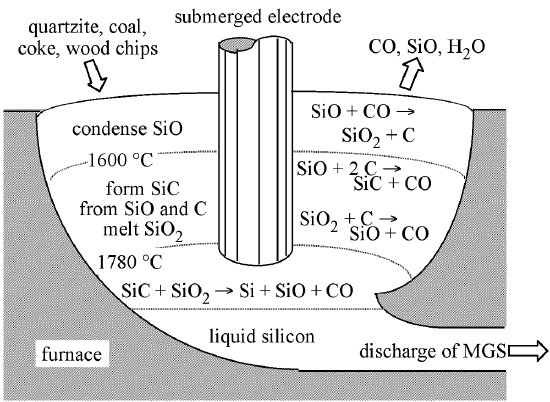
The overall reduction reaction of SiO2 is expressed in (7.10.1), however, the reaction sequence is more complex than this overall reaction implies, and involves the formation of SiC and SiO intermediates. The initial reaction between molten SiO2 and C, (7.10.2), takes place in the arc between adjacent electrodes, where the local temperature can exceed 2000 °C. The SiO and CO thus generated flow to cooler zones in the furnace where SiC is formed, (7.10.3), or higher in the bed where they reform SiO2 and C, (7.10.2). The SiC reacts with molten SiO2, (7.10.4), producing the desired silicon along with SiO and CO. The molten silicon formed is drawn-off from the furnace and solidified.
\[ \text{SiO}_2\text{(liquid) + 2 C(solid)} \rightarrow \text{Si(liquid) + 2 CO(gas)} \nonumber \]
\[ \text{SiO}_2\text{ + 2 C} \xrightleftharpoons[\text{<1600 °C}]{\text{>1700 °C}} \text{SiO + CO} \nonumber \]
\[ \text{SiO + 2C} \rightarrow \text{SiC + CO (1600 - 1700 °C)} \nonumber \]
\[ \text{SiC _ SiO}_2 \rightarrow \text{Si + SiO + CO} \nonumber \]
The as-produced MGS is approximately 98-99% pure, with the major impurities being aluminum and iron (Table \(\PageIndex{1}\)), however, obtaining low levels of boron impurities is of particular importance, because it is difficult to remove and serves as a dopant for silicon. The drawbacks of the above process are that it is energy and raw material intensive. It is estimated that the production of one metric ton (1,000 kg) of MGS requires 2500 - 2700 kg quartzite, 600 kg charcoal, 600 - 700 kg coal or coke, 300 - 500 kg wood chips, and 500,000 kWh of electric power. Currently, approximately 500,000 metric tons of MGS are produced per year, worldwide. Most of the production (ca. 70%) is used for metallurgical applications (e.g., aluminum-silicon alloys are commonly used for automotive engine blocks) from whence its name is derived. Applications in a variety of chemical products such as silicone resins account for about 30%, and only 1% or less of the total production of MGS is used in the manufacturing of high-purity EGS for the electronics industry. The current worldwide consumption of EGS is approximately 5 x 10⁶ kg per year.
Electronic-grade silicon (EGS)
Electronic-grade silicon (EGS) is a polycrystalline material of exceptionally high purity and is the raw material for the growth of single-crystal silicon. EGS is one of the purest materials commonly available, see Table \(\PageIndex{2}\). The formation of EGS from MGS is accomplished through chemical purification processes. The basic concept of which involves the conversion of MGS to a volatile silicon compound, which is purified by distillation, and subsequently decomposed to re-form elemental silicon of higher purity (i.e., EGS). Irrespective of the purification route employed, the first step is physical pulverization of MGS followed by its conversion to the volatile silicon compounds.
A number of compounds, such as monosilane (SiH4), dichlorosilane (SiH2Cl2), trichlorosilane (SiHCl3), and silicon tetrachloride (SiCl4), have been considered as chemical intermediates. Among these, SiHCl3 has been used predominantly as the intermediate compound for subsequent EGS formation, although SiH4 is used to a lesser extent. Silicon tetrachloride and its lower chlorinated derivatives are used for the chemical vapor deposition (CVD) growth of Si and SiO2. The boiling points of silane and its chlorinated products (Table \(\PageIndex{3}\)) are such that they are conveniently separated from each other by fractional distillation.
| Compound | Boiling point (°C) |
|---|---|
| SiH4 | -112.3 |
| SiH3Cl | -30.4 |
| SiH2Cl2 | 8.3 |
| SiHCl3 | 31.5 |
| SiCl4 | 57.6 |
The reasons for the predominant use of SiHCl3 in the synthesis of EGS are as follows:
- SiHCl3 can be easily formed by the reaction of anhydrous hydrogen chloride with MGS at reasonably low temperatures (200 - 400 °C);
- it is liquid at room temperature so that purification can be accomplished using standard distillation techniques;
- it is easily handled and if dry can be stored in carbon steel tanks;
- its liquid is easily vaporized and, when mixed with hydrogen it can be transported in steel lines without corrosion;
- it can be reduced at atmospheric pressure in the presence of hydrogen;
- its deposition can take place on heated silicon, thus eliminating contact with any foreign surfaces that may contaminate the resulting silicon; and
- it reacts at lower temperatures (1000 - 1200 °C) and at faster rates than does SiCl4.
Chlorosilane (Seimens) process
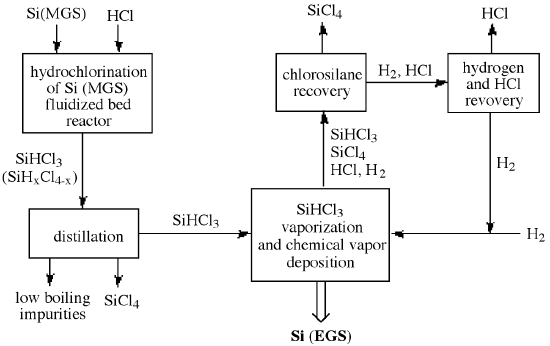
Trichlorosilane is synthesized by heating powdered MGS with anhydrous hydrogen chloride (HCl) at around 300 °C in a fluidized-bed reactor, (7.10.5).
\[ \text{Si(solid_ + 3 HCl(gas)} \xrightleftharpoons[\text{>900 °C}]{\text{ca. 300 °C}} \text{SiHCl}_3\text{(vapor) + H}_2\text{(gas)} \nonumber \]
Since the reaction is actually an equilibrium and the formation of SiHCl3 highly exothermic, efficient removal of generated heat is essential to assure a maximum yield of SiHCl3. While the stoichiometric reaction is that shown in (7.10.5), a mixture of chlorinated silanes is actually prepared which must be separated by fractional distillation, along with the chlorides of any impurities. In particular iron, aluminum, and boron are removed as FeCl3 (b.p. = 316 °C), AlCl3 (m.p. = 190 °C subl.), and BCl3 (b.p. = 12.65 °C), respectively. Fractional distillation of SiHCl3 from these impurity halides result in greatly increased purity with a concentration of electrically active impurities of less than 1 ppb.
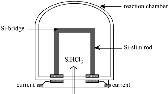
EGS is prepared from purified SiHCl3 in a chemical vapor deposition (CVD) process similar to the epitaxial growth of Si. The high-purity SiHCl3 is vaporized, diluted with high-purity hydrogen, and introduced into the Seimens deposition reactor, shown schematically in Figure \(\PageIndex{2}\). Within the reactor, thin silicon rods called slim rods (ca. 4 mm diameter) are supported by graphite electrodes. Resistance heating of the slim rods causes the decomposition of the SiHCl3 to yield silicon, as described by the reverse reaction shown in (7.10.5).
The shift in the equilibrium from forming SiHCl3 from Si at low temperature, to forming Si from SiHCl3 at high temperature is as a consequence of the temperature dependence, (7.10.6), of the equilibrium constant, (7.10.7) where ρ = partial pressure, for (7.10.5). Since the formation of SiHCl3 is exothermic, i.e., ΔH < 0, an increase in the temperature causes the partial pressure of SiHCl3 to decrease. Thus, the Siemens process is typically run at ca. 1100 °C, while the reverse fluidized bed process is carried out at 300 °C.
\[ \text{lnK}_{\text{p}} \text{ = } \dfrac{ \text{-}\Delta\text{H}}{\text{RT}} \nonumber \]
\[ \text{K}_{\text{p}} \text{ = } \dfrac{^{\rho}\text{SiHCl}_3 \text{ } ^{\rho}\text{H}_2}{^{\rho}\text{HCl}} \nonumber \]
The slim rods act as a nucleation point for the deposition of silicon, and the resulting polycrystalline rod consists of columnar grains of silicon (polysilicon) grown perpendicular to the rod axis. Growth occurs at less than 1 mm per hour, and after deposition for 200 to 300 hours high-purity (EGS) polysilicon rods of 150 - 200 mm in diameter are produced. For subsequent float-zone refining the polysilicon EGS rods are cut into long cylindrical rods. Alternatively, the as-formed polysilicon rods are broken into chunks for single crystal growth processes, for example Czochralski melt growth.
In addition to the formation of silicon, the HCl coproduct reacts with the SiHCl3 reactant to form silicon tetrachloride (SiCl4) and hydrogen as major byproducts of the process, (7.10.8). This reaction represents a major disadvantage with the Seimens process: poor efficiency of silicon and chlorine consumption. Typically, only 30% of the silicon introduced into CVD reactor is converted into high-purity polysilicon.
\[ \text{HCl + SiHCl}_3 \rightarrow \text{SiCl}_4\text{ + H}_2 \nonumber \]
In order to improve efficiency the HCl, SiCl4, H2, and unreacted SiHCl3 are separated and recovered for recycling. Figure \(\PageIndex{3}\) illustrates the entire chlorosilane process starting with MGS and including the recycling of the reaction byproducts to achieve high overall process efficiency. As a consequence, the production cost of high-purity EGS depends on the commercial usefulness of the byproduct, SiCl4. Additional disadvantages of the Seimens process are derived from its relatively small batch size, slow growth rate, and high power consumption. These issues have lead to the investigation of alternative cost efficient routes to EGS.
Silane process
An alternative process for the production of EGS that has begun to receive commercial attention is the pyrolysis of silane (SiH4). The advantages of producing EGS from SiH4 instead of SiHCl3 are potentially lower costs associated with lower reaction temperatures, and less harmful byproducts. Silane decomposes < 900 °C to give silicon and hydrogen, (7.10.9).
\[\text{SiH}_4\text{(vapor)} \rightarrow \text{Si(solid) + 2 H}_2\text{(gas)} \nonumber \]
Silane may be prepared by a number of routes, each having advantages with respect to purity and production cost. The simplest process involves the direct reaction of MGS powders with magnesium at 500 °C in a hydrogen atmosphere, to form magnesium silicide (Mg2Si). The magnesium silicide is then reacted with ammonium chloride in liquid ammonia below 0 °C, (7.10.10).
\[ \text{Mg}_2\text{Si + 4 NH}_4\text{Cl} \rightarrow \text{SiH}_4\text{ + 2 MgCl}_2\text{ + 5 NH}_3 \nonumber \]
This process is ideally suited to the removal of boron impurities (a p-type dopant in Si), because the diborane (B2H6) produced during the reaction forms the Lewis acid-base complex, H3B(NH3), whose volatility is sufficiently lower than SiH4, allowing for the purification of the latter. It is possible to prepare EGS with a boron content of ≤ 20 ppt using SiH4 synthesized in this manner. However, phosphorus (another dopant) in the form of PH3 may be present as a contaminant requiring subsequent purification of the SiH4.
Alternative routes to SiH4 involve the chemical reduction of SiCl4 by either lithium hydride, (7.10.11), lithium aluminum hydride, (7.10.12), or via hydrogenation in the presence of elemental silicon, (7.10.13) - (7.10.16). The hydride reduction reactions may be carried-out on relatively large scales (ca. 50 kg), but only batch processes. In contrast, Union Carbide has adapted the hydrogenation to a continuous process, involving disproportionation reactions of chlorosilanes, (7.10.14) - (7.10.16), and the fractional distillation of silane, Table \(\PageIndex{3}\).
\[ \text{SiCl}_4\text{ + LiH} \rightarrow \text{SiH}_4\text{ + 4 LiCl} \nonumber \]
\[ \text{SiCl}_4\text{ + LiAlH}_4 \rightarrow \text {SiH}_4 \text{ + LiCl + AlCl}_4 \nonumber \]
\[ \text{SiCl}_4\text{ + 2 H}_2\text{ + Si(98%)} \rightarrow \text{4 SiHCl}_3 \nonumber \]
\[ \text{2 SiHCl}_3 \rightarrow \text{SiH}_2\text{Cl}_2\text{ + 2 SiHCl}_3 \nonumber \]
\[ \text{3 SiH}_2\text{Cl}_2 \rightarrow \text{SiH}_2\text{Cl + 2 SiHCl}_3 \nonumber \]
\[ \text{2 SiH}_3\text{Cl} \rightarrow \text{SiH}_4\text{ + SiH}_2\text{Cl}_2 \nonumber \]
Pyrolysis of silane on resistively heated polysilicon filaments at 700 - 800 °C yields polycrystalline EGS. As noted above, the EGS formed has remarkably low boron impurities compared with material prepared from trichlorosilane. Moreover, the resulting EGS is less contaminated with transition metals from the reactor container because SiH4 decomposition does not cause as much of a corrosion problem as is observed with halide precursor compounds.
Granular polysilicon deposition
Both the chlorosilane (Seimens) and silane processes result in the formation of rods of EGS. However, there has been increased interest in the formation of granular polycrystalline EGS. This process was developed in 1980’s, and relies on the decomposition of SiH4 in a fluidized-bed deposition reactor to produce free-flowing granular polysilicon.
Tiny silicon particles are fluidized in a SiH4/H2 flow, and act as seed crystal onto which polysilicon deposits to form free-flowing spherical particles. The size distribution of the particles thus formed is over the range from 0.1 to 1.5 mm in diameter with an average particle size of 0.7 mm. The fluidized-bed seed particles are originally made by grinding EGS in a ball (or hammer) mill and leaching the product with acid, hydrogen peroxide, and water. This process is time-consuming and costly, and tended to introduce undesirable impurities from the metal grinders. In a new method, large EGS particles are fired at each other by a high-speed stream of inert gas and the collision breaks them down into particles of suitable size for a fluidized bed. This process has the main advantage that it introduces no foreign materials and requires no leaching or other post purification.
The fluidized-bed reactors are much more efficient than traditional rod reactors as a consequence of the greater surface area available during CVD growth of silicon. It has been suggested that fluidized-bed reactors require 1/5 to 1/10 the energy, and half the capital cost of the traditional process. The quality of fluidized-bed polysilicon has proven to be equivalent to polysilicon produced by the conventional methods. Moreover, granular EGS in a free-flowing form, and with high bulk density, enables crystal growers to obtain the high, reproducible production yields out of each crystal growth run. For example, in the Czochralski crystal growth process, crucibles can be quickly and easily filled to uniform loading with granular EGS, which typically exceed those of randomly stacked polysilicon chunks produced by the Siemens silane process.
Zone refining
The technique of zone refining is used to purify solid materials and is commonly employed in metallurgical refining. In the case of silicon may be used to obtain the desired ultimate purity of EGS, which has already been purified by chemical processes. Zone refining was invented by Pfann, and makes use of the fact that the equilibrium solubility of any impurity (e.g., Al) is different in the solid and liquid phases of a material (e.g., Si). For the dilute solutions, as is observed in EGS silicon, an equilibrium segregation coefficient (k0) is defined by k0 = Cs/Cl, where Cs and Cl are the equilibrium concentrations of the impurity in the solid and liquid near the interface, respectively.
If k0 is less than 1 then the impurities are left in the melt as the molten zone is moved along the material. In a practical sense a molten zone is established in a solid rod. The zone is then moved along the rod from left to right. If k0 < 1 then the frozen part left on the trailing edge of the moving molten zone will be purer than the material that melts in on the right-side leading edge of the moving molten zone. Consequently the solid to the left of the molten zone is purer than the solid on the right. At the completion of the first pass the impurities become concentrated to the right of the solid sample. Repetition of the process allows for purification to exceptionally high levels. Table \(\PageIndex{4}\) lists the equilibrium segregation coefficients for common impurity and dopant elements in silicon; it should be noted that they are all less than 1.
| Element | k0 | Element | k0 |
|---|---|---|---|
| aluminum | 0.002 | iron | 8 x 10⁻⁶ |
| boron | 0.8 | oxygen | 0.25 |
| carbon | 0.07 | phosphorus | 0.35 |
| copper | 4 x 10⁻⁶ | antimony | 0.023 |
Bibliography
- K. G. Baraclough, K. G., in The Chemistry of the Semiconductor Industry, Eds. S. J. Moss and A. Ledwith, Blackie and Sons, Glasgow, Scotland (1987).
- L. D. Crossman and J. A. Baker, Semiconductor Silicon 1977, Electrochem. Soc., Princeton, New Jersey (1977).
- W. C. O’Mara, Ed. Handbook of Semiconductor Silicon Technology, Noyes Pub., New Jersey (1990).
- W. G. Pfann, Zone Melting, John Wiley & Sons, New York, (1966).
- F. Shimura, Semiconductor Silicon Crystal Technology, Academic Press (1989).