
10.2: Measuring Key Transport Properties of FET Devices
- Page ID
- 55937

\( \newcommand{\vecs}[1]{\overset { \scriptstyle \rightharpoonup} {\mathbf{#1}} } \)
\( \newcommand{\vecd}[1]{\overset{-\!-\!\rightharpoonup}{\vphantom{a}\smash {#1}}} \)
\( \newcommand{\id}{\mathrm{id}}\) \( \newcommand{\Span}{\mathrm{span}}\)
( \newcommand{\kernel}{\mathrm{null}\,}\) \( \newcommand{\range}{\mathrm{range}\,}\)
\( \newcommand{\RealPart}{\mathrm{Re}}\) \( \newcommand{\ImaginaryPart}{\mathrm{Im}}\)
\( \newcommand{\Argument}{\mathrm{Arg}}\) \( \newcommand{\norm}[1]{\| #1 \|}\)
\( \newcommand{\inner}[2]{\langle #1, #2 \rangle}\)
\( \newcommand{\Span}{\mathrm{span}}\)
\( \newcommand{\id}{\mathrm{id}}\)
\( \newcommand{\Span}{\mathrm{span}}\)
\( \newcommand{\kernel}{\mathrm{null}\,}\)
\( \newcommand{\range}{\mathrm{range}\,}\)
\( \newcommand{\RealPart}{\mathrm{Re}}\)
\( \newcommand{\ImaginaryPart}{\mathrm{Im}}\)
\( \newcommand{\Argument}{\mathrm{Arg}}\)
\( \newcommand{\norm}[1]{\| #1 \|}\)
\( \newcommand{\inner}[2]{\langle #1, #2 \rangle}\)
\( \newcommand{\Span}{\mathrm{span}}\) \( \newcommand{\AA}{\unicode[.8,0]{x212B}}\)
\( \newcommand{\vectorA}[1]{\vec{#1}} % arrow\)
\( \newcommand{\vectorAt}[1]{\vec{\text{#1}}} % arrow\)
\( \newcommand{\vectorB}[1]{\overset { \scriptstyle \rightharpoonup} {\mathbf{#1}} } \)
\( \newcommand{\vectorC}[1]{\textbf{#1}} \)
\( \newcommand{\vectorD}[1]{\overrightarrow{#1}} \)
\( \newcommand{\vectorDt}[1]{\overrightarrow{\text{#1}}} \)
\( \newcommand{\vectE}[1]{\overset{-\!-\!\rightharpoonup}{\vphantom{a}\smash{\mathbf {#1}}}} \)
\( \newcommand{\vecs}[1]{\overset { \scriptstyle \rightharpoonup} {\mathbf{#1}} } \)
\( \newcommand{\vecd}[1]{\overset{-\!-\!\rightharpoonup}{\vphantom{a}\smash {#1}}} \)
\(\newcommand{\avec}{\mathbf a}\) \(\newcommand{\bvec}{\mathbf b}\) \(\newcommand{\cvec}{\mathbf c}\) \(\newcommand{\dvec}{\mathbf d}\) \(\newcommand{\dtil}{\widetilde{\mathbf d}}\) \(\newcommand{\evec}{\mathbf e}\) \(\newcommand{\fvec}{\mathbf f}\) \(\newcommand{\nvec}{\mathbf n}\) \(\newcommand{\pvec}{\mathbf p}\) \(\newcommand{\qvec}{\mathbf q}\) \(\newcommand{\svec}{\mathbf s}\) \(\newcommand{\tvec}{\mathbf t}\) \(\newcommand{\uvec}{\mathbf u}\) \(\newcommand{\vvec}{\mathbf v}\) \(\newcommand{\wvec}{\mathbf w}\) \(\newcommand{\xvec}{\mathbf x}\) \(\newcommand{\yvec}{\mathbf y}\) \(\newcommand{\zvec}{\mathbf z}\) \(\newcommand{\rvec}{\mathbf r}\) \(\newcommand{\mvec}{\mathbf m}\) \(\newcommand{\zerovec}{\mathbf 0}\) \(\newcommand{\onevec}{\mathbf 1}\) \(\newcommand{\real}{\mathbb R}\) \(\newcommand{\twovec}[2]{\left[\begin{array}{r}#1 \\ #2 \end{array}\right]}\) \(\newcommand{\ctwovec}[2]{\left[\begin{array}{c}#1 \\ #2 \end{array}\right]}\) \(\newcommand{\threevec}[3]{\left[\begin{array}{r}#1 \\ #2 \\ #3 \end{array}\right]}\) \(\newcommand{\cthreevec}[3]{\left[\begin{array}{c}#1 \\ #2 \\ #3 \end{array}\right]}\) \(\newcommand{\fourvec}[4]{\left[\begin{array}{r}#1 \\ #2 \\ #3 \\ #4 \end{array}\right]}\) \(\newcommand{\cfourvec}[4]{\left[\begin{array}{c}#1 \\ #2 \\ #3 \\ #4 \end{array}\right]}\) \(\newcommand{\fivevec}[5]{\left[\begin{array}{r}#1 \\ #2 \\ #3 \\ #4 \\ #5 \\ \end{array}\right]}\) \(\newcommand{\cfivevec}[5]{\left[\begin{array}{c}#1 \\ #2 \\ #3 \\ #4 \\ #5 \\ \end{array}\right]}\) \(\newcommand{\mattwo}[4]{\left[\begin{array}{rr}#1 \amp #2 \\ #3 \amp #4 \\ \end{array}\right]}\) \(\newcommand{\laspan}[1]{\text{Span}\{#1\}}\) \(\newcommand{\bcal}{\cal B}\) \(\newcommand{\ccal}{\cal C}\) \(\newcommand{\scal}{\cal S}\) \(\newcommand{\wcal}{\cal W}\) \(\newcommand{\ecal}{\cal E}\) \(\newcommand{\coords}[2]{\left\{#1\right\}_{#2}}\) \(\newcommand{\gray}[1]{\color{gray}{#1}}\) \(\newcommand{\lgray}[1]{\color{lightgray}{#1}}\) \(\newcommand{\rank}{\operatorname{rank}}\) \(\newcommand{\row}{\text{Row}}\) \(\newcommand{\col}{\text{Col}}\) \(\renewcommand{\row}{\text{Row}}\) \(\newcommand{\nul}{\text{Nul}}\) \(\newcommand{\var}{\text{Var}}\) \(\newcommand{\corr}{\text{corr}}\) \(\newcommand{\len}[1]{\left|#1\right|}\) \(\newcommand{\bbar}{\overline{\bvec}}\) \(\newcommand{\bhat}{\widehat{\bvec}}\) \(\newcommand{\bperp}{\bvec^\perp}\) \(\newcommand{\xhat}{\widehat{\xvec}}\) \(\newcommand{\vhat}{\widehat{\vvec}}\) \(\newcommand{\uhat}{\widehat{\uvec}}\) \(\newcommand{\what}{\widehat{\wvec}}\) \(\newcommand{\Sighat}{\widehat{\Sigma}}\) \(\newcommand{\lt}{<}\) \(\newcommand{\gt}{>}\) \(\newcommand{\amp}{&}\) \(\definecolor{fillinmathshade}{gray}{0.9}\)Field Effect Transistors
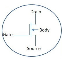
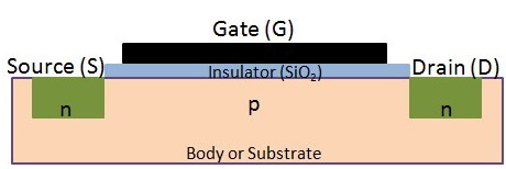
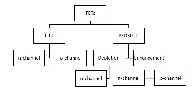
Arguably the most important invention of modern times, the transistor was invented in 1947 at Bell Labs by John Bardeen, William Shockley, and Walter Brattain. The result of efforts to replace inefficient and bulky vacuum tubes in current regulation and switching functions. Further advances in transistor technology led to the field effect transistors (FETs), the bedrock of modern electronics. FETs operate by utilizing an electric field to control the flow of charge carriers along a channel, analogous to a water valve to control the flow of water in your kitchen sink. The FET consists of 3 terminals, a source (S), drain (D), and gate (G). The region between the source and drain is called the channel. The conduction in the channel depends on the availability of charge carriers controlled by the gate voltage. Figure depicts a typical schematic and Figure \(\PageIndex{1}\) the associated cross-section of a FET with the source, draing and gate terminals labeled. FETs come in a variety of flavors depending on their channel doping (leading to enhancement and depletion modes) and gate types, as seen in Figure \(\PageIndex{2}\). The two FET types are junction field effect transistors (JFETs) and metal oxide semiconductor field effect transistors (MOSFETs).
JFET Fundamentals
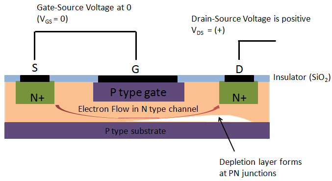
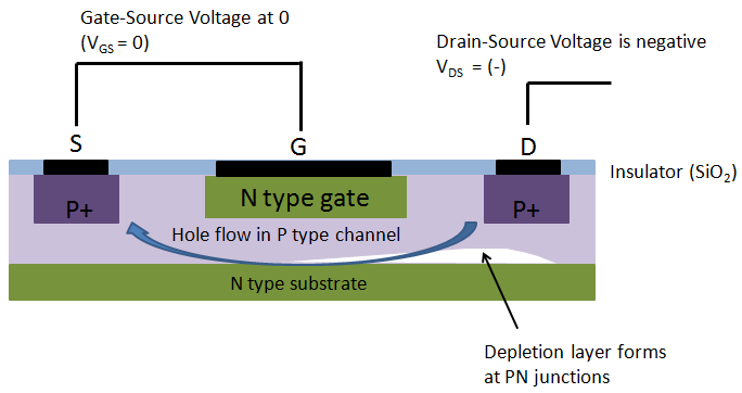
Junction field effect transistors (JFETs) as their name implies utilize a PN-junction to control the flow of charge carriers. The PN-junction is formed when opposing doping schemes are broght together on both sides of the channel. The doping schemes can be made to be either n-type (electrons) or p-type (holes) by doping with boron/gallium or phosphorus/arsenic respectively. The n-channel JFETs consists of pnp junctions where the source and drain are n-doped and the gate is p-doped. Figure \(\PageIndex{4}\) shows the cross section of a n-channel JFET in the “ON” state obtained by applying a positive drain-source voltage in the absence of a gate-source voltage. Alternatively the p-channel JFET consists of npn junctions where the source and drain are p-doped and the gate is n-doped. For p-channel a negative drain-source voltage is applied in the absence of a gate voltage to turn “ON” the npn device, as seen in Figure \(\PageIndex{5}\). Since JFETs are “ON” when no gate-source voltage is applied they are called depletion mode devices. Meaning that a depletion region is required to turn “OFF” the device. This is where the PN-junction comes into play. The PN-junction works by enabling a depletion region to form where electrons and holes combine leaving behind positive and negative ions which inhibit further charge transfer as well as depleting the availability of charge carriers at the interface. This depletion region is pushed further into the channel by applying a gate-source voltage. If the voltage is sufficient the depletion region on either side of the channel will “pinch off” the flow through the channel and the device will be “OFF”. This voltage is called the pinch off voltage, VP. The n-channel VP is obtained by increasing the gate-source voltage in the negative direction, while the p-channel VP is obtained by increasing the gate-source voltage in the positive direction.
MOSFET Fundamentals
The metal oxide semiconductor field effect transistor (MOSFET) utilizes an oxide layer (typically SiO2) to isolate the gate from the source and drain. The thin layer of oxide prevents flow of current to the gate, but enables an electric field to be applied to the channel which regulates the flow of charge carriers through the channel.MOSFETs unlike JFETs can operate in depletion or enhancement mode characterized by their ON or OFF state at zero gate-source voltage, VGS.
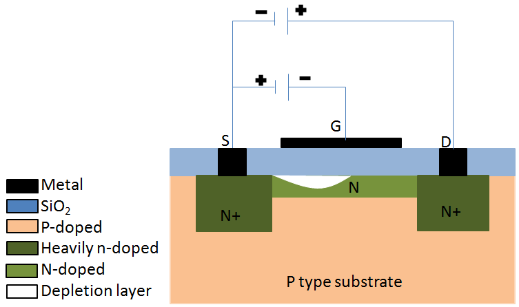
For depletion mode MOSFETs the device is “ON” when the VGS is zero as a result of the devices structure and doping scheme. The n-channel depletion mode MOSFET consists of heavily n-doped source and drain terminals on top of a p-doped substrate. Underneath an insulating oxide layer there is a thin layer of n-type silicon which allows charge carriers to flow in the absence of a gate voltage. When a negative voltage is applied to the gate a depletion region forms inside the channel, as seen in Figure. If the gate voltage is sufficient the depletion region pinches off the flow of electrons.
For enhancement mode MOSFETs the ON state is attained by applying a gate voltage in the direction of the drain voltage; a positive voltage for n-channel enhancement MOSFETs, and a negative voltage for p-channel enhancement MOSFETs. The term “enhancement” is derived from the increase in conductivity seen by applying a gate voltage. This increase in conductivity is enabled by an inversion layer induced by the applied electric field at the gate as shown in Figure \(\PageIndex{7}\) for n-channel enhancement mode MOSFETs and Figure \(\PageIndex{8}\) for p-channel enhancement mode MOSFETs respectively.
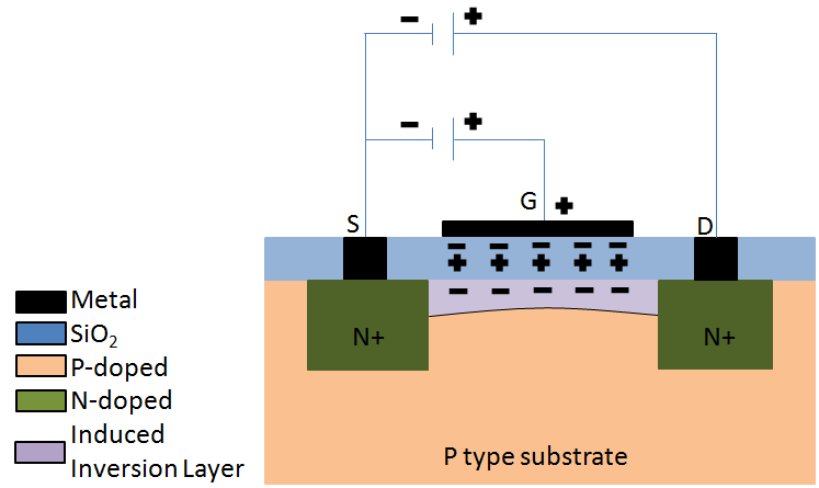
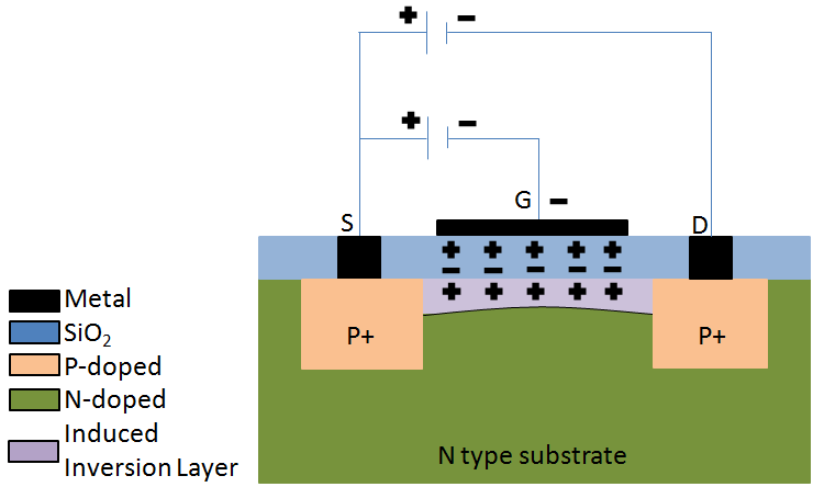
The thickness of this inversion layer is controlled by the magnitude of the gate voltage. The minimum voltage required to form the inversion layer is called the gate-to-source threshold voltage, VT. In the case of n-channel enhancement mode MOSFETs, the “ON” state is reached when VGS > VT and a positive drain-source voltage, VDS, is applied. If the VGS is too low, then increasing the VDS further results only in increasing the depletion region around the drain. The p-channel enhancement mode MOSFETs operate similarly except that the voltages are reversed. Specifically, the “ON” state occurs when VGS < VT and a negative drain-source voltage is applied.
Measurement of key FET Parameters
In both an academic and industrial setting characterization of FETs is beneficial for determining device performance. Identifying the quality and type of FET can easily be addressed by measuring the transport characteristics under different experimental conditions utilizing a semiconductor characterization system (SCS). By analyzing the V-I characteristics through what are called voltage sweeps, the following key device parameters can be determined:
Pinch off Voltage Vp
The voltage needed to turn “OFF” a JFET. When designing circuits it is essential that the pinch-off voltage be determined to avoid current leakage which can dramatically reduce performance.
Threshold Voltage VT
The voltage needed to turn “ON” a MOSFET. This is a critical parameter in effective circuit design.
Channel Resistance RDS
The resistance between the drain and source in the channel. This influences the amount of current being transferred between the two terminals.
Power Dissipation PD
The power dissipation determines the amount of heat generated by the transistor. This becomes a real problem since the transport properties deteriorate as the channel is heated.
Effective Charge Carrier Mobility µn
The charge carrier mobility determines how quickly the charge carrier can move through the channel. In most cases higher mobility leads to better device performance. The mobility can also be used to gauge the impurity, defect, temperature, and charge carrier concentrations.
Transconductance gain gm (transfer admittance)
The gm is a measure of gain or amplification of a current for a given change in gate voltage. This is critical for amplification type electronics.
Equipment Needs
PC with Keithley Interactive Test Environment (KITE) software.
Semiconductor characterization system (Keithley 4200-SCS or equivalent).
Probe station.
Probe tips.
Protective gloves.
Measurement (V-I) Characteristics
The Semiconductor Characterization System is an automated system that provides both (V-I) and (V-C) characterization of semiconductor devices and test structures. The advanced digital sweep parameter analyzer provides sub-micron characterization with accuracy and speed. This system utilizes the Keithley Interactive Test Environment (KITE) software designed specifically for semiconductor characterization.
Procedure
- Connect the probe tips to the probe station. Then attach the banana plugs from the probe station to the BNC connector, making sure not to connect to ground.
- Select the appropriate connections for your test from Table \(\PageIndex{1}\)
- Place your transistor sample on the probe station, but don’t let the probe tips touch the sample to prevent possible electric shock(during power up, the SMU may momentarily output high voltage).
- Turn on power located on the lower right of the front panel. The power up sequence may take up to 2 minutes.
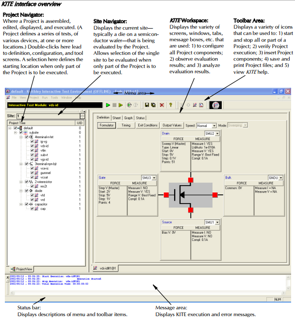
- Start KITE software. Figure \(\PageIndex{9}\) shows the interface window.
- Select the appropriate setup from the Project Tree drop down (top left).
- Match the Definition tab terminal connections to the physical connections of probe tips. If connection is not yet matched you can assign/reassign the terminal connections by using the arrow key next to the instrument selection box that displays a list of possible connections. Select the connection in the instrument selection box that matches the physical connection of the device terminal.
- Set the Force Measure settings for each terminal. Fill in the necessary function parameters such as start, stop, step size, range, and compliance. For typical voltage sweeps you’ll want to force the voltage between the drain and source while measuring the current at the drain. Make sure to conduct several voltage sweeps at various forced gate voltages to aid in the analysis.
- Check the current box/voltage box if you desire the current/voltage to be recorded in the Sheet tab Data worksheet and be available for plotting in the Graph tab.
- Now make contact to your sample with the probe tips
- Run the measurement setup by clicking the green Run arrow on the tool bar located above the Definition tab. Make sure the measuring indicator light at bottom right hand corner of the front panel is lit.
- Save data by clicking on the Sheet tab then selecting the Save As tab. Select the file format and location.
| Connection | Description |
| SMU1 | Medium power with low noise preamplifier |
| SMU2 | Medium power source without preamplifier |
| SMU3 | High Power |
| GNRD | For large currents |
Measurement Analysis
Typical V-I Characteristics of JFETs
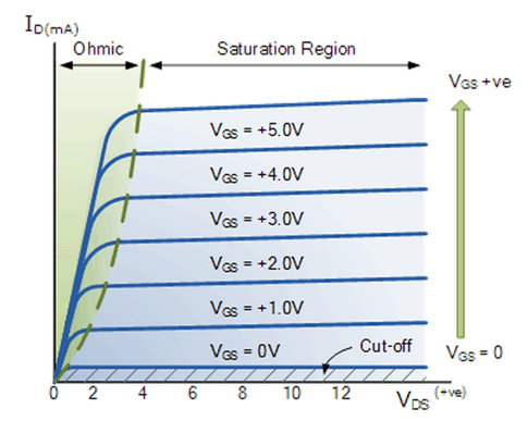
Voltage sweeps are a great way to learn about the device. Figure \(\PageIndex{10}\) shows a typical plot of drain-source voltage sweeps at various gate-source voltages while measuring the drain current, ID for a n-channel JFET. The V-I characteristics have four distinct regions. Analysis of these regions can provides critical information about the device characteristics such as the pinch off voltage, VP, transcunductance gain, gm, drain-source channel resistance, RDS, and power dissipation, PD.

Ohmic Region (Linear Region)
This region is bounded by VDS < VP. Here the JFET begins to flow a drain current with a linear response to the voltage, behaving like a variable resistor. In this region the drain-source channel resistance, RDS is modeled by \ref{1}, where ΔVDS is the change in drain-source voltage, ΔID is the change in drain current, and gm is the transcunductance gain. Solving for gm results in \ref{2}.
\[ R_{DS}\ =\ \frac{\Delta V_{DS}}{\Delta I_{D}}\ =\ \frac{1}{g_{m}} \label{1} \]
\[ g_m\ =\ \frac{\Delta I_{D}}{\Delta V_{DS}}\ =\ \frac{1}{R_{DS}} \label{2} \]
Saturation Region
This is the region where the JFET is completely “ON”. The maximum amount of current is flowing for the given gate-source voltage. In this region the drain current can be modeled by the \ref{3}, where ID is the drain current, IDSS is the maximum current, VGS is the gate-source voltage, and VP is the pinch off voltage. Solving for the pinch off voltage results in \ref{4}.
\[ I_{D}\ =\ I_{DSS}(1\ -\ \frac{V_{GS}}{V_{P}}) \label{3} \]
\[ V_{P}\ =\ 1\ -\ \frac{V_{GS}}{\sqrt{\frac{I_D}{I_{DSS}}}} \label{4} \]
Breakdown Region
This region is characterized by the sudden increase in current. The drain-source voltage supplied exceeds the resistive limit of the semiconducting channel, resulting in the transistor to break down and flow an uncontrolled current.
Pinch-off Region (Cutoff Region)
In this region the gate-source voltage is sufficient to restrict the flow through the channel, in effect cutting off the drain current. The power dissipation, PD, can be solved utilizing Ohms law (I = V/R) for any region using \ref{5}.
\[ P_{D}\ =\ I_{D}\ \times \ V_{DC}\ =\ (I_{D})^{2}\ \times \ R_{DS}\ =\ (V_{DS})^{2}/R_{DS} \label{5} \]
The p-channel JFET V-I characteristics behave similarly except that the voltages are reversed. Specifically, the pinch off point is reached when the gate-source voltage is increased in a positive direction, and the saturation region is met when the drain-source voltage is increased in the negative direction.
Typical V-I Characteristics of MOSFETs
Figure \(\PageIndex{11}\) shows a typical plot of drain-source voltage sweeps at various gate-source voltages while measuring the drain current, ID for an ideal n-channel enhancement MOSFET. Like JFETs, the V-I characteristics of MOSFETS have distinct regions that provide valuable information about device transport properties.
Ohmic Region (Linear Region)
The n-channel enhanced MOSFET behaves linearly, acting like a variable resistor, when the gate-source voltage is greater than the threshold voltage and the drain-source voltage is greater than the gate-source voltage. In this region the drain current can be modeled by \ref{6}, where ID is the drain current, VGS is the gate-source voltage, VT is the threshold voltage, VDS is the drain-source voltage, and k is the geometric factor described by \ref{7}, where µn is the charge-carrier effective mobility, COX is the gate oxide capacitance, W is the channel width, and L is the channel length.
\[ I_{D}\ =\ 2k{(V_{GS}-V_{T})V_{DS}\ -\ [(V_{DS})^{2}/2]} \label{6} \]
\[ k\ =\ \mu _{n} C_{OX} \frac{W}{L} \label{7} \]
Saturation Region
In this region the MOSFET is considered fully “ON”. The drain current for the saturation region is modeled by \ref{8}. The drain current is mainly influenced by the gate-source voltage, while the drain-source voltage has no effect.
\[ I_{D}\ =\ k(V_{GS}\ -\ V_{T})^{2} \label{8} \]
Solving for the threshold voltage VT results in \ref{9}.
\[ V_{T}\ =\ V_{GS}\ -\ \sqrt{\frac{I_{D}}{k}} \label{9} \]
Pinch-off Region (Cutoff Region)
When the gate-source voltage, VGS, is below the threshold voltage VT the charge carriers in the channel are not available “cutting off” the charge flow. Power dissipation for MOSFETs can also be solved using equation 6 in any region as in the JFET case.
FET V-I Summary
The typical I-V characteristics for the whole family of FETs seen in Figure \(\PageIndex{11}\) are plotted in Figure \(\PageIndex{12}\).
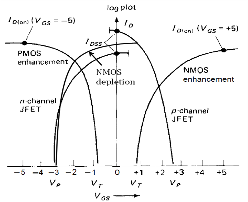
From Figure \(\PageIndex{12}\) we can see how the doping schemes that lead to enhancement and depletion are displaced along the VGS axis. In addition, from the plot the ON or OFF state can be determined for a given gate-source voltage, where (+) is positive, (0) is zero, and (-) is negative, as seen in Table \(\PageIndex{1}\).
| FET Type | VGS = (-) | VGS = 0 | VGS = (+) |
|---|---|---|---|
| n-channel JFET | OFF | ON | ON |
| p-channel JFET | ON | ON | OFF |
| n-channel depletion MOSFET | OFF | ON | ON |
| p-channel depletion MOSFET | ON | ON | OFF |
| n-channel enhancement MOSFET | OFF | OFF | ON |
| p-channel enhancement MOSFET | ON | ON | OFF |