
Scanning electron microscopy (SEM)
- Page ID
- 148465
\( \newcommand{\vecs}[1]{\overset { \scriptstyle \rightharpoonup} {\mathbf{#1}} } \)
\( \newcommand{\vecd}[1]{\overset{-\!-\!\rightharpoonup}{\vphantom{a}\smash {#1}}} \)
\( \newcommand{\dsum}{\displaystyle\sum\limits} \)
\( \newcommand{\dint}{\displaystyle\int\limits} \)
\( \newcommand{\dlim}{\displaystyle\lim\limits} \)
\( \newcommand{\id}{\mathrm{id}}\) \( \newcommand{\Span}{\mathrm{span}}\)
( \newcommand{\kernel}{\mathrm{null}\,}\) \( \newcommand{\range}{\mathrm{range}\,}\)
\( \newcommand{\RealPart}{\mathrm{Re}}\) \( \newcommand{\ImaginaryPart}{\mathrm{Im}}\)
\( \newcommand{\Argument}{\mathrm{Arg}}\) \( \newcommand{\norm}[1]{\| #1 \|}\)
\( \newcommand{\inner}[2]{\langle #1, #2 \rangle}\)
\( \newcommand{\Span}{\mathrm{span}}\)
\( \newcommand{\id}{\mathrm{id}}\)
\( \newcommand{\Span}{\mathrm{span}}\)
\( \newcommand{\kernel}{\mathrm{null}\,}\)
\( \newcommand{\range}{\mathrm{range}\,}\)
\( \newcommand{\RealPart}{\mathrm{Re}}\)
\( \newcommand{\ImaginaryPart}{\mathrm{Im}}\)
\( \newcommand{\Argument}{\mathrm{Arg}}\)
\( \newcommand{\norm}[1]{\| #1 \|}\)
\( \newcommand{\inner}[2]{\langle #1, #2 \rangle}\)
\( \newcommand{\Span}{\mathrm{span}}\) \( \newcommand{\AA}{\unicode[.8,0]{x212B}}\)
\( \newcommand{\vectorA}[1]{\vec{#1}} % arrow\)
\( \newcommand{\vectorAt}[1]{\vec{\text{#1}}} % arrow\)
\( \newcommand{\vectorB}[1]{\overset { \scriptstyle \rightharpoonup} {\mathbf{#1}} } \)
\( \newcommand{\vectorC}[1]{\textbf{#1}} \)
\( \newcommand{\vectorD}[1]{\overrightarrow{#1}} \)
\( \newcommand{\vectorDt}[1]{\overrightarrow{\text{#1}}} \)
\( \newcommand{\vectE}[1]{\overset{-\!-\!\rightharpoonup}{\vphantom{a}\smash{\mathbf {#1}}}} \)
\( \newcommand{\vecs}[1]{\overset { \scriptstyle \rightharpoonup} {\mathbf{#1}} } \)
\(\newcommand{\longvect}{\overrightarrow}\)
\( \newcommand{\vecd}[1]{\overset{-\!-\!\rightharpoonup}{\vphantom{a}\smash {#1}}} \)
\(\newcommand{\avec}{\mathbf a}\) \(\newcommand{\bvec}{\mathbf b}\) \(\newcommand{\cvec}{\mathbf c}\) \(\newcommand{\dvec}{\mathbf d}\) \(\newcommand{\dtil}{\widetilde{\mathbf d}}\) \(\newcommand{\evec}{\mathbf e}\) \(\newcommand{\fvec}{\mathbf f}\) \(\newcommand{\nvec}{\mathbf n}\) \(\newcommand{\pvec}{\mathbf p}\) \(\newcommand{\qvec}{\mathbf q}\) \(\newcommand{\svec}{\mathbf s}\) \(\newcommand{\tvec}{\mathbf t}\) \(\newcommand{\uvec}{\mathbf u}\) \(\newcommand{\vvec}{\mathbf v}\) \(\newcommand{\wvec}{\mathbf w}\) \(\newcommand{\xvec}{\mathbf x}\) \(\newcommand{\yvec}{\mathbf y}\) \(\newcommand{\zvec}{\mathbf z}\) \(\newcommand{\rvec}{\mathbf r}\) \(\newcommand{\mvec}{\mathbf m}\) \(\newcommand{\zerovec}{\mathbf 0}\) \(\newcommand{\onevec}{\mathbf 1}\) \(\newcommand{\real}{\mathbb R}\) \(\newcommand{\twovec}[2]{\left[\begin{array}{r}#1 \\ #2 \end{array}\right]}\) \(\newcommand{\ctwovec}[2]{\left[\begin{array}{c}#1 \\ #2 \end{array}\right]}\) \(\newcommand{\threevec}[3]{\left[\begin{array}{r}#1 \\ #2 \\ #3 \end{array}\right]}\) \(\newcommand{\cthreevec}[3]{\left[\begin{array}{c}#1 \\ #2 \\ #3 \end{array}\right]}\) \(\newcommand{\fourvec}[4]{\left[\begin{array}{r}#1 \\ #2 \\ #3 \\ #4 \end{array}\right]}\) \(\newcommand{\cfourvec}[4]{\left[\begin{array}{c}#1 \\ #2 \\ #3 \\ #4 \end{array}\right]}\) \(\newcommand{\fivevec}[5]{\left[\begin{array}{r}#1 \\ #2 \\ #3 \\ #4 \\ #5 \\ \end{array}\right]}\) \(\newcommand{\cfivevec}[5]{\left[\begin{array}{c}#1 \\ #2 \\ #3 \\ #4 \\ #5 \\ \end{array}\right]}\) \(\newcommand{\mattwo}[4]{\left[\begin{array}{rr}#1 \amp #2 \\ #3 \amp #4 \\ \end{array}\right]}\) \(\newcommand{\laspan}[1]{\text{Span}\{#1\}}\) \(\newcommand{\bcal}{\cal B}\) \(\newcommand{\ccal}{\cal C}\) \(\newcommand{\scal}{\cal S}\) \(\newcommand{\wcal}{\cal W}\) \(\newcommand{\ecal}{\cal E}\) \(\newcommand{\coords}[2]{\left\{#1\right\}_{#2}}\) \(\newcommand{\gray}[1]{\color{gray}{#1}}\) \(\newcommand{\lgray}[1]{\color{lightgray}{#1}}\) \(\newcommand{\rank}{\operatorname{rank}}\) \(\newcommand{\row}{\text{Row}}\) \(\newcommand{\col}{\text{Col}}\) \(\renewcommand{\row}{\text{Row}}\) \(\newcommand{\nul}{\text{Nul}}\) \(\newcommand{\var}{\text{Var}}\) \(\newcommand{\corr}{\text{corr}}\) \(\newcommand{\len}[1]{\left|#1\right|}\) \(\newcommand{\bbar}{\overline{\bvec}}\) \(\newcommand{\bhat}{\widehat{\bvec}}\) \(\newcommand{\bperp}{\bvec^\perp}\) \(\newcommand{\xhat}{\widehat{\xvec}}\) \(\newcommand{\vhat}{\widehat{\vvec}}\) \(\newcommand{\uhat}{\widehat{\uvec}}\) \(\newcommand{\what}{\widehat{\wvec}}\) \(\newcommand{\Sighat}{\widehat{\Sigma}}\) \(\newcommand{\lt}{<}\) \(\newcommand{\gt}{>}\) \(\newcommand{\amp}{&}\) \(\definecolor{fillinmathshade}{gray}{0.9}\)Student author: Emily Nagle 2019
How SEM works
In an SEM, an electron beam is emitted from an electron gun, then narrowed to a size of approximately 0.4-5 nm in diameter through the use of one or two condenser lenses. The beam then passes through a pair of deflection coils in the electron column to deflect the beam in the x and y axes before interacting with the sample. This deflection ensures that the scan is in a raster fashion, which means it is a rectangular image capture pattern of the sample. When the electron beam interacts with the sample, it loses energy due to random scattering and absorption by the sample. A schematic showing the components of SEM and how it works is shown in Figure 1. Additionally, a video explaining how SEM works is provided.
.svg?revision=1)
Figure \(\PageIndex{1}\): Schematic of how an SEM works (Figure courtesy of Creative Commons license and can be found at
https://en.Wikipedia.org/wiki/File:Schema_MEB_(en).svg)
Video \(\PageIndex{1}\): Illustration of how SEM works coutresy of Creative Commons license and found at
https://en.Wikipedia.org/wiki/File:Scanning_Electron_Microscope.ogv#filehistory
The electron beam of a scanning electron microscope interacts with atoms at different depths within the sample to produce different signals including secondary electrons, back-scattered electrons, and characteristic X-rays. Each of these signals has its own detector in the SEM, as seen in Figure 1. Secondary electrons are low energy electrons that are ejected from the valence or conduction bands of atoms in the sample through inelastic scattering from the beam electrons. Back-scattered electrons are electrons from the beam that are reflected through elastic scattering interactions with atoms in the sample. The intensity of the back-scattered electron signal is dependent upon the atomic number so it can provide information about the distribution of different elements in a sample. The characteristic X-rays are emitted when the electron beam interacts with the sample and removes an inner shell electron, resulting in a higher-energy electron filling the shell and releasing energy. The energy or wavelength of these X-rays can be measured by Energy-dispersive X-Ray Spectroscopy to identify and measure the abundance and distribution of elements in the sample. The electron beam absorbed by the sample is detected and used to create an image of the sample distribution. The resulting image is a map displaying the intensity of signal emitted from the area of the sample being scanned, as seen in Figure 2. Additionally, EDS detectors can be attached to the SEM for elemental analysis.
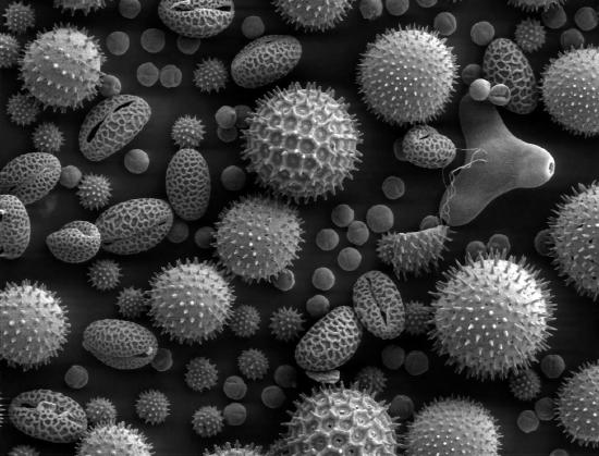
Figure \(\PageIndex{2}\): SEM image of pollen grains. Image released to the public domain by original author Dartmouth College Electron Microscope Facility and found at https://upload.wikimedia.org/Wikipedia/commons/a/a4/Misc_pollen.jpg
In order to obtain SEM images, the sample must be electrically conductive at the surface as well as electrically grounded so that it does not accumulate charge. Samples are mounted onto the specimen holder using a conductive adhesive. Metal samples require minimal sample preparation other than conductively mounting the sample to the stage. Non-conductive materials typically undergo ultrathin coating with electrically conductive materials such as gold, platinum, chromium, or graphite. The coating is accomplished through sputter-coating or evaporation under high vacuum.
How to Interpret the Data
Different SEM images can be produced based on the type of detector being used and these image can be used to see what the sample looks like on the nanoscale. The most typical detector used detects the secondary electrons that are emitted from the sample by inelastic scattering. The number of secondary electrons detected represents the signal intensity and is combined with the position of the beam to produce a gray-scale images showing the sample's topography, as seen in Figure 2. Back-scattered electrons can also be used to get an image since elements will reflect a different number of electrons. Therefore, the intensity of back-scattered electrons will vary throughout a sample depending on the elements present. An SEM image produced from the intensity of back-scattered electrons and the beam position can show the distribution of different elements in the sample. Elements that are heavier and reflect more electrons will appear brighter in the image so back-scattered electrons can show contrasts in chemical composition. However, the identity of the different elements cannot be determined with SEM alone, an EDS attachment would have to be used to quantify the relative abundance of different elements.
Good Literature Examples
Works Cited
Useful Resources for In-Depth Reading
- McMullan, D. Scanning electron microscopy 1928-1965. Scanning 17, 175–185 (2006).
- Smith, K. C. A. & Oatley, C. W. The scanning electron microscope and its fields of application. Br. J. Appl. Phys. 6, 391–399 (1955).
- https://www.atascientific.com.au/sem-imaging-applications-practical-uses-scanning-electron-microscopes/