
Detectors
- Page ID
- 202093
\( \newcommand{\vecs}[1]{\overset { \scriptstyle \rightharpoonup} {\mathbf{#1}} } \)
\( \newcommand{\vecd}[1]{\overset{-\!-\!\rightharpoonup}{\vphantom{a}\smash {#1}}} \)
\( \newcommand{\dsum}{\displaystyle\sum\limits} \)
\( \newcommand{\dint}{\displaystyle\int\limits} \)
\( \newcommand{\dlim}{\displaystyle\lim\limits} \)
\( \newcommand{\id}{\mathrm{id}}\) \( \newcommand{\Span}{\mathrm{span}}\)
( \newcommand{\kernel}{\mathrm{null}\,}\) \( \newcommand{\range}{\mathrm{range}\,}\)
\( \newcommand{\RealPart}{\mathrm{Re}}\) \( \newcommand{\ImaginaryPart}{\mathrm{Im}}\)
\( \newcommand{\Argument}{\mathrm{Arg}}\) \( \newcommand{\norm}[1]{\| #1 \|}\)
\( \newcommand{\inner}[2]{\langle #1, #2 \rangle}\)
\( \newcommand{\Span}{\mathrm{span}}\)
\( \newcommand{\id}{\mathrm{id}}\)
\( \newcommand{\Span}{\mathrm{span}}\)
\( \newcommand{\kernel}{\mathrm{null}\,}\)
\( \newcommand{\range}{\mathrm{range}\,}\)
\( \newcommand{\RealPart}{\mathrm{Re}}\)
\( \newcommand{\ImaginaryPart}{\mathrm{Im}}\)
\( \newcommand{\Argument}{\mathrm{Arg}}\)
\( \newcommand{\norm}[1]{\| #1 \|}\)
\( \newcommand{\inner}[2]{\langle #1, #2 \rangle}\)
\( \newcommand{\Span}{\mathrm{span}}\) \( \newcommand{\AA}{\unicode[.8,0]{x212B}}\)
\( \newcommand{\vectorA}[1]{\vec{#1}} % arrow\)
\( \newcommand{\vectorAt}[1]{\vec{\text{#1}}} % arrow\)
\( \newcommand{\vectorB}[1]{\overset { \scriptstyle \rightharpoonup} {\mathbf{#1}} } \)
\( \newcommand{\vectorC}[1]{\textbf{#1}} \)
\( \newcommand{\vectorD}[1]{\overrightarrow{#1}} \)
\( \newcommand{\vectorDt}[1]{\overrightarrow{\text{#1}}} \)
\( \newcommand{\vectE}[1]{\overset{-\!-\!\rightharpoonup}{\vphantom{a}\smash{\mathbf {#1}}}} \)
\( \newcommand{\vecs}[1]{\overset { \scriptstyle \rightharpoonup} {\mathbf{#1}} } \)
\(\newcommand{\longvect}{\overrightarrow}\)
\( \newcommand{\vecd}[1]{\overset{-\!-\!\rightharpoonup}{\vphantom{a}\smash {#1}}} \)
\(\newcommand{\avec}{\mathbf a}\) \(\newcommand{\bvec}{\mathbf b}\) \(\newcommand{\cvec}{\mathbf c}\) \(\newcommand{\dvec}{\mathbf d}\) \(\newcommand{\dtil}{\widetilde{\mathbf d}}\) \(\newcommand{\evec}{\mathbf e}\) \(\newcommand{\fvec}{\mathbf f}\) \(\newcommand{\nvec}{\mathbf n}\) \(\newcommand{\pvec}{\mathbf p}\) \(\newcommand{\qvec}{\mathbf q}\) \(\newcommand{\svec}{\mathbf s}\) \(\newcommand{\tvec}{\mathbf t}\) \(\newcommand{\uvec}{\mathbf u}\) \(\newcommand{\vvec}{\mathbf v}\) \(\newcommand{\wvec}{\mathbf w}\) \(\newcommand{\xvec}{\mathbf x}\) \(\newcommand{\yvec}{\mathbf y}\) \(\newcommand{\zvec}{\mathbf z}\) \(\newcommand{\rvec}{\mathbf r}\) \(\newcommand{\mvec}{\mathbf m}\) \(\newcommand{\zerovec}{\mathbf 0}\) \(\newcommand{\onevec}{\mathbf 1}\) \(\newcommand{\real}{\mathbb R}\) \(\newcommand{\twovec}[2]{\left[\begin{array}{r}#1 \\ #2 \end{array}\right]}\) \(\newcommand{\ctwovec}[2]{\left[\begin{array}{c}#1 \\ #2 \end{array}\right]}\) \(\newcommand{\threevec}[3]{\left[\begin{array}{r}#1 \\ #2 \\ #3 \end{array}\right]}\) \(\newcommand{\cthreevec}[3]{\left[\begin{array}{c}#1 \\ #2 \\ #3 \end{array}\right]}\) \(\newcommand{\fourvec}[4]{\left[\begin{array}{r}#1 \\ #2 \\ #3 \\ #4 \end{array}\right]}\) \(\newcommand{\cfourvec}[4]{\left[\begin{array}{c}#1 \\ #2 \\ #3 \\ #4 \end{array}\right]}\) \(\newcommand{\fivevec}[5]{\left[\begin{array}{r}#1 \\ #2 \\ #3 \\ #4 \\ #5 \\ \end{array}\right]}\) \(\newcommand{\cfivevec}[5]{\left[\begin{array}{c}#1 \\ #2 \\ #3 \\ #4 \\ #5 \\ \end{array}\right]}\) \(\newcommand{\mattwo}[4]{\left[\begin{array}{rr}#1 \amp #2 \\ #3 \amp #4 \\ \end{array}\right]}\) \(\newcommand{\laspan}[1]{\text{Span}\{#1\}}\) \(\newcommand{\bcal}{\cal B}\) \(\newcommand{\ccal}{\cal C}\) \(\newcommand{\scal}{\cal S}\) \(\newcommand{\wcal}{\cal W}\) \(\newcommand{\ecal}{\cal E}\) \(\newcommand{\coords}[2]{\left\{#1\right\}_{#2}}\) \(\newcommand{\gray}[1]{\color{gray}{#1}}\) \(\newcommand{\lgray}[1]{\color{lightgray}{#1}}\) \(\newcommand{\rank}{\operatorname{rank}}\) \(\newcommand{\row}{\text{Row}}\) \(\newcommand{\col}{\text{Col}}\) \(\renewcommand{\row}{\text{Row}}\) \(\newcommand{\nul}{\text{Nul}}\) \(\newcommand{\var}{\text{Var}}\) \(\newcommand{\corr}{\text{corr}}\) \(\newcommand{\len}[1]{\left|#1\right|}\) \(\newcommand{\bbar}{\overline{\bvec}}\) \(\newcommand{\bhat}{\widehat{\bvec}}\) \(\newcommand{\bperp}{\bvec^\perp}\) \(\newcommand{\xhat}{\widehat{\xvec}}\) \(\newcommand{\vhat}{\widehat{\vvec}}\) \(\newcommand{\uhat}{\widehat{\uvec}}\) \(\newcommand{\what}{\widehat{\wvec}}\) \(\newcommand{\Sighat}{\widehat{\Sigma}}\) \(\newcommand{\lt}{<}\) \(\newcommand{\gt}{>}\) \(\newcommand{\amp}{&}\) \(\definecolor{fillinmathshade}{gray}{0.9}\)Spectroscopy is the study of how light interacts with matter, and a necessity for these studies is the ability to detect light. To do this, spectroscopists use a wide variety of detectors, which are devices that convert incident photons into a measurable signal. Presented here is a discussion of the fundamental concepts that define a detector, and an examination of several detectors commonly used in spectroscopy.
Introduction
All spectroscopic measurements are made through the use of a detector, which converts photons into a measurable signal. A ubiquitous example of a photon detector is the human eye, which can detect visible light with wavelengths in the range of ~390-700 nanometers. Some of the earliest non-biological photon detectors were photographic plates, in which absorbed photons cause chemical reactions that manifest as color changes in the film. A vast majority of modern detectors act as photon transducers, which transform electromagnetic radiation into electrical signals which can be amplified and processed for final interpretation. The manner by which photons are converted to electrical signals varies widely, but detectors can be divided into two broad categories: those that function via the photoelectric effect, and those that are based on the solid-state properties of semiconductors.
The photoelectric effect is a physical phenomenon through which absorbed photons can eject electrons from the surface of a conductor, provided the photons have energies greater than the work function of the material. The kinetic energy of the ejected electron, termed a photoelectron, is given by
\[KE_{electron} = h\nu - \phi\]
in which \(h\) is Planck's constant, \(\nu\) is the frequency of the incident photons, and \(\phi\) is the work function. Many detectors exploit this effect, as the ejected photoelectrons can be collected at an anode and measured as a current.
Semiconductor-based detectors rely on a similar effect, though instead of ejecting photoelectrons from the surface of a conductor, absorbed photons excite electrons from the valence band of a semiconductor into the conduction band. This excitation results in an electon-hole pair, which allows current to flow through the semiconductor; this current can be quantified and interpreted with an appropriate circuit.
Fundamental Characteristics of Detectors
All detectors can be evaluated in terms of their various fundamental characteristics, including spectral response, linearity, quantum efficiency, dynamic range, response time, and susceptibility to noise. Certain types of detectors are better suited to particular applications based on how well they perform in these areas.
Spectral Response and Linearity
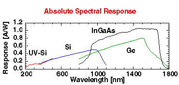
The ideal detector would be able to convert incident photons of any energy into an electrical signal, and would have a perfectly linear response, such that the magnitude of the current produced is directly proportional to the number of photons striking the detector. The spectral response of a real detector is limited to a fairly small region of the electromagnetic spectrum, and the response can deviate significantly from linearity, as shown in Figure 1. The spectral response of a detector largely determines its usefulness for various applications; silicon photodiodes are used in the UV and visible regions but are not sensitive beyond 1100 nm, while germanium photodiodes are insensitive to UV light, but can detect longer wavelengths up to 1800 nm.
Quantum Efficiency
Quantum efficiency is a measure of how well a detector can convert photons into an electrical signal. It is often reported as the ratio, \(\eta\), of the number of electrons generated by the detector divided by the number of incident photons, but can also be reported as the percent of incident photons that will be translated into a measurable signal; the latter definition takes into account the effects of noise and other signal losses within the system, and represents a more accurate measure of the efficiency of a detector. An ideal detector would have a quantum efficiency of 100%, and there exist several types of real detectors that approach this limit, with the ability to detect the absorption of single photons.
Dynamic Range
The dynamic range of a detector is a measure of its ability to generate a reliable signal relative to the intensity of incident radiation. A detector with a very high dynamic range will be able to measure both extremely weak and extremely strong photon sources, but this is often connected to a decrease in overall sensitivity. As the range of measurable intensities increases, the ratio of a signal to the maximum possible signal becomes smaller, which leads to a smaller change in signal for the same incident intensity, and thus a lower sensitivity. Conversely, extremely sensitive detectors tend to have relatively small dynamic ranges; the photomultiplier tube, which is capable of detecting single photons, can be easily damaged or destroyed when exposed to even moderate levels of incident radiation.
Response Time
The generation of an electrical signal from an incident photon occurs on a very fast, but measurable timescale, which varies by detector type. The response time is the amount of time necessary before a detector is able to generate another signal; the faster the response time, the more quickly variations in incident radiation can be resolved. An ideal detector would have zero response time, though this is an impossibility in real detectors. Some detectors, such as photodiode arrays, which use multiple detector elements arranged to gather spatial information, can have response times on the order of milliseconds, whereas conventional photocathode detectors have response times on the order of nanoseconds. Specialized detectors, such a streak cameras, can have temporal resolutions as low as 0.5 picoseconds, allowing for the study of extremely short-lived events.
Noise
All detectors generate small signals that do not correspond to absorption of a photon, and these signals are collectively termed noise. Noise does not contain any useful information, and therefore it is important to minimize signals due to noise relative to the overall signal; the higher the signal-to-noise ratio, the more sensitive the detector. There are many forms of noise, including shot noise, dark current noise, thermal noise, generation-recombination noise, and read-out noise, all of which arise from different factors. Various detectors are more or less susceptible to certain types of noise, and both experimental conditions and detector design can be modified to reduce noise to a minimum.
Shot Noise
Shot noise is a direct consequense of the discrete nature of photons, and how a detector generates a discrete number of photoelectrons through its interaction with photons. In any counting experiment of \(N\) trials, the standard deviation associated with the measurement is \(\sqrt{N}\). In photon detectors, the signal is directly proportional to the number of incident photons, and the associated uncertainty in this measurement arises from the statistical probability of whether or not a photoelectron will be emitted when a photon is absorbed. This uncertainty gives rise to random fluctuations in the signal, and manifests as noise. Therefore, when \(N\) photons are incident on a detector, the signal-to-noise ratio is:
\[\frac{signal}{noise} = \frac{N}{\sqrt{N}}\times \frac{\sqrt{N}}{\sqrt{N}}=\frac{N\sqrt{N}}{N}=\sqrt{N}\]
In detectors with quantum efficiencies less than unity, the shot noise is slightly greater than this value, but in most experiments the number of incident photons is very large, and thus the signal-to-noise ratio is also large, making the shot noise imperceptibly small when compared to the overall signal. Shot noise is present in all measurements, due to the quantum nature of light, and is not dependent on temperature or the energy of the photon absorbed. Shot noise only becomes a significant contributor to overall noise when the number of incident photons is extremely small, such as in single-photon-counting experiments, and when other forms of noise are almost entirely eliminated.
Thermal Noise
Thermal noise, also known as Johnson-Nyquist noise, is intrinsic to all conductive materials, regardless of relative conductivity or applied voltage. The band structure of conductors allows for the free motion of charge carriers; the random motions of the charge carriers produce small current fluctuations in the system, which appear as a Gaussian distribution on top of the overall signal. As the speed with which these charge carriers move is proportional to temperature of the system, thermal noise can be significantly reduced by lowering the temperature of the detector.
Dark Current Noise
Dark current noise is the current generated by photon detectors in the complete absence of photons. This type of noise is also thermally generated, but instead of current fluctuations due to the random motion of charge carriers, dark current noise is created by thermionic emission of electrons from photocathodes, or thermal generation of electron-hole pairs within a semiconductor. In the case of photocathodes, thermionic electrons are indistinguishable from photoelectrons, and are measured as an additional current on top of the photon-induced current. In the case of semiconductors, the generation of electron-hole pairs changes the conductivity of the semiconductor, and more current can flow through the circuit; when the pairs recombine, the conductivity drops to its initial value. This manifests as a fluctuation of the measured current above and below the real signal. In both cases, the event that generate the noise are discrete, such that dark current noise has the same properties as shot noise; unlike shot noise, however, dark currents are thermally generated, and can be significantly reduced by cooling the system.
Generation-Recombination Noise
Another form of noise affecting only semiconductor-based detectors is generation-recombination noise. Generation-recombination noise arises from the fact that when photons excite photoelectrons in a semiconductor, the number of electron-hole pairs generated fluctuates due to the statistical probability of the excitation occuring. The relative number of electron-hole pairs changes the conductivity of the semiconductor, which gives rise to current fluctuations similar to those created by dark current, with characteristics of shot noise. However, generation-recombination noise is not thermally generated, and cannot be reduced by cooling the system.
Read-Out Noise
Read-out noise is only a factor in detectors that integrate signals, such as charge coupled devices (CCDs) and complementary metal-oxide-semiconductor (CMOS) sensors. These detectors collect and store charge over an extended period of time, and when the charge collection is complete, the accumulated charge is "read off" the collection grid, a process which involves moving packets of charge between multiple electrodes for measurement, or converting charge signals into voltages using operational amplifiers. Each movement or conversion of a packet is subject to the gain or loss of a small number of electrons, and the changes in the number of electrons in each packet give rise to the read-out noise. Read-out noise is not dependent on temperature, but increases with the number of packet movements or conversions, as well as the speed with which the packets are moved and read.
Types of Detectors
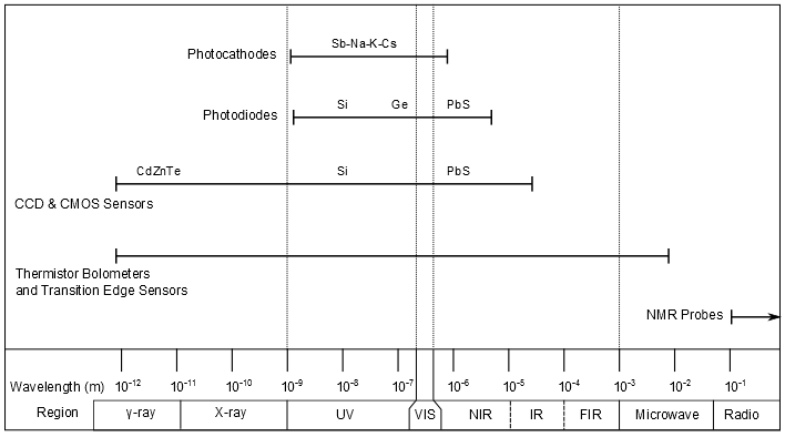
The number of types of detectors and their variants employed in spectroscopy is exceedingly large, with new detectors constantly being developed for better performance characteristics and use in novel sensing applications. As can be seen in Figure 2, different types of detectors are sensitive to different regions of the electromagnetic spectrum, and the region of interest may dictate which detector type is utilized. Here, a selection of some of the more common detectors are discussed in more detail, including the design, function, and performance of each.
Scintillators
While not technically photon detectors by themselves, scintillators are an integral component in many types of detectors, especially of high-energy photons, and it is instructive to understand what they are and how they work before discussing their use in conjunction with other technologies. A scintillator is a material that absorbs a photon of a given energy, and then undergoes fluorescence, re-emitting a photon of a lower energy. In this way, scintillators can be used to absorb photons that fall outside the normal energy range of a detector, and re-emit photons of wavelengths that can be detected.
Many scintillators used in photon detectors employ crystalline inorganic compounds, each of which have characteristic sensitivities, emission wavelengths, and relaxations times. For example, the most commonly used scintillator material is NaI(Tl), crystalline sodium iodide doped with thallium. This compound has a peak fluorescence of 415 nm, a relaxation time of 250 nanoseconds, and emits 38 photons per keV gamma ray absorbed. A newer alternative is LaBr3(Ce), lanthanum bromide doped with cerium, which has nearly double the efficiency of NaI(Tl), and a relaxation time of only 16 nanoseconds. However, LaBr3(Ce) is much more expensive, and is extremely hygroscopic, requiring special handling to protect the scintillator from moisture.
Photocathodes and Photomultiplier Tubes
Photocathodes
Photocathodes are among the simplest photon detectors, relying on only the photoelectric effect to generate a signal. A photon strikes and is absorbed by the photocathode, ejecting a photoelectron in the process. This photoelectron is accelerated through an electric field and is collected at an anode, where it is read as a current. In actual construction, the photocathode is a low work function metal, which is held at a positive potential relative to the collection anode. This assembly is usually housed in a vacuum tube, to limit the interference of air and water vapor and to increase the mean free path of the electrons, thus increasing the quantum efficiency of the detector.
Photocathodes are generally sensitive to radiation from ~180-900 nm, though certain materials are capable of detecting near IR light up to 1600 nm. The most common materials used as photocathodes for broadband spectrometers are multi-alkali alloys of antimony, such as Sb-Na-K-Cs, which is sensitive to photons of energies ranging from vacuum UV to near IR. In addition to their fairly broad spectral response, photocathodes also exhibit very large dynamic ranges, and have a nearly linear response across the entire range. Furthermore, photocathodes have response times on the order of 1-2 nanoseconds, and are only subject to small amounts of shot noise and thermal noise. However, noise from dark current can become a problem for particularly low work function photocathodes, as thermionic emission of electrons can generate current in the absence of photons. Additionally, their overall sensitivity is quite limited, as there is no internal signal gain in the detector. An external amplifier can be used to increase the magnitude of the signal, but this does not improve the signal-to-noise ratio, and generates a certain amount of noise itself.
Photomultiplier Tubes
Photomultiplier tubes (PMTs) are the direct successors to photocathodes, and function in exactly the same way with one key difference: instead of accelerating photoelectrons directly to the anode, a PMT amplifies the number of photoelectrons through the use of a dynode chain. A dynode, usually made from BeO or MgO, is held at a positive potential, such that when it is struck by a single energetic electron, the dynode will emit several electrons. The next dynode in the chain is held at a slightly lower potential, such that an electric field accelerates electrons liberated from the first dynode towards the second, where the electrons again liberate additional electrons. The process continues in a cascading fashion until the final anode is reached; if 6-8 dynodes are chained together, then a single photoelectron incident on the first can generate 106-108 electrons at the anode.

This method of amplification overcomes a number of problems inherent in conventional photocathodes. The primary advantage of a PMT is the dramatically increased sensitivity due to the internal signal gain; modern PMTs are capable of reliably detecting single photons. Additionally, through the use of the high-voltage dynode chain, the signal is amplified but thermal noise is not, as thermal noise is independent of applied voltage. In this sense, the thermal noise is diminished to essentially nothing, and the signal becomes shot noise dominated, allowing the detector to reach theoretical limits of sensitivity, with a quantum efficiency of 100%, provided that the dark current is minimized by lowering the temperature of the system.
PMTs respond best when used to detect radiation in the UV and visible regions, but they are used as detectors in a wide variety of instruments, from gamma and X-ray spectrometers to near IR spectrometers. This is possible through the use of a variety of scintillators, discussed above, placed between the incoming photons and the photocathode. Scintillators are capable of converting higher energy photons into visible photons, which can be efficiently amplified by the PMT. With a modest decrease in response time and a slight increase in noise, the addition of a scintillator allows for the superior sensitivity and signal of a PMT in spectral regions where they would otherwise be insensitive.
Photodiodes and Photodiode Arrays
Photodiodes and Arrays
Photodiodes exemplify the simplest of the solid-state detectors, and are built upon semiconductor p-n junctions. An individual p-n junction is constructed from the union of a positively-doped material with a negatively-doped material, and contact between the two surfaces results in the local motion of major charge carriers. Electrons near the junction drift towards the p-type material, and holes drift towards the n-type material, resulting in a depletion zone that has an intrinsic electric field, which creates a potential barrier across the junction.
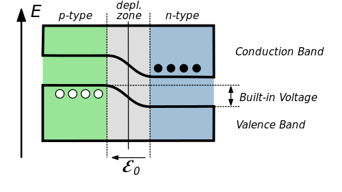
This junction is known as a diode, and will allow current to flow through it in only one direction. When the diode is subjected to an external potential, called a bias, the energies of the p- and n-type materials are shifted relative to each other, changing the magnitude of the potential barrier. When a positive voltage is applied to the p-type side and a negative voltage to the n-type side, the holes in the p-type and the electrons in the n-type sides are forced into the depletion zone. This is known as a forward bias, and when it is large enough, the depletion zone and its potential barrier will disappear and the diode will allow current to flow through it. However, if the potentials are reversed, into what is called a reverse bias, the electrons in the n-type side and the holes in the p-type side are pulled away from each other, widening the depletion zone, and increasing the potential barrier across the junction, preventing current from flowing through the diode.
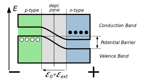
In photodiode detectors, the diode is held under reverse bias, which maintains a fairly large electric field throughout the depletion zone that will sweep free electrons towards the anode and free holes towards the cathode. When a diode is illuminated with electromagnetic radiation with energy sufficient to excite an electron from the valence band to the conduction band of the semiconductor, electron-hole pairs are generated. As these electron-hole pairs are separated and accelerated in opposite directions by the electric field, a photocurrent is produced, by which the incident radiation can be quantified.
The spectral response of a photodiode can be tuned to different regions by carefully selecting the materials used to make the p-n junction. For example, silicon-based photodiodes are sensitive to radiation between 190-1100 nm, making them useful for UV, visible, and limited near-IR spectroscopies, while lead sulfide photodiodes are sensitive in the range of ~1000-3500 nm, enabling detection in both near-IR and short-wave-IR. Additionally, solid-state photodiodes provide a very nearly linear response throughout a large dynamic range. These properties, coupled with the fact that photodiodes do not require high-voltage power supplies and are physically small, relatively inexpensive to manufacture, and much more robust than photocathodes makes them an excellent choice for use in many spectroscopic instruments.
One additional advantage that stems from the small size of photodiodes is the ability to arrange multiple detectors into an array, known as a photodiode array (PDA). These arrays can take any shape and contain any number of detector elements, but are often arranged in a linear fashion, enabling the detection and encoding of spatial data as well as the energy and intensity of the incident light. As these arrays can be read out in parallel, a PDA has the same response time as an individual detector, allowing for the collection of much more data with the same response time.
However, there are certain aspects of photodiode detectors, such as overall sensitivity, response time, and noise levels, that prevent them from being completely superior to photocathode technologies. Conventionally operated photodiodes, even with quantum efficiencies around 80%, do not have any internal gain, and thus cannot compete with photomultiplier tubes in terms of the ability to detect very small numbers of photons. Furthermore, photodiodes generally have slower response times than similar photocathode detectors, on the order of microseconds, as there is a small but significant time-lag for the electron-hole pairs to be swept from the depletion zone to the electrical contacts. Finally, while shot, thermal, and dark current noise is present in all detectors, photodiodes are also subject to generation-recombination noise, though most photodiodes are limited by thermal noise and dark current noise. Many photodiode detectors must be cooled to reduce overall noise to acceptable levels.
Avalanche Photodiodes
One improvement can be made to photodiode detectors to bring their overall sensitivity into the same range as conventional photomultiplier tubes. When a diode held in reverse bias is subjected to a critical overpotential, the diode will break down and allow current to flow across it; this critical voltage is referred to as the breakdown voltage. In the absence of current, a photodiode can be held at a potential well above the breakdown voltage (known as being operated in Geiger mode), such that as soon as a photon is absorbed and an electron-hole pair generated, the diode will undergo breakdown and allow current to flow in the reverse direction. In order to achieve the sensitivity of a PMT, there must be significant internal signal gain, and this is realized through what is called an avalanche breakdown. The electron and hole generated by the absorption of a photon are accelerated very rapidly towards the cathode and anode by the very high potential difference across the photodiode. The electron and hole can gain enough kinetic energy that they are capable of causing impact ionizations within the semiconductor, generating additional electron-hole pairs. As each new pair is generated, they too are accelerated towards the electrodes, and cause additional ionizations; this chain reaction results in an avalanche of electrons moving towards the cathode and holes moving towards the anode, such that when they arrive, a very intense current pulse is measured. In this way, single photon absorptions can be detected in much the same way that they can with PMTs, but with a much lower overall voltage requirement. Where avalanche photodiodes still cannot compete with conventional PMTs is in response time; as the avalanche breakdown in a photodiode is a self-sustaining event, it must be stopped, or quenched, by lowering the potential across the junction to well below the breakdown voltage, and then raised back up before another absorption can be detected. This effectively means that while time resolution for single-photon events can be very good, on the order of 0.6 nanoseconds, it can take 10s of nanoseconds to reset the detector to a useable state, compared to the 1-2 nanosecond response times of PMTs.
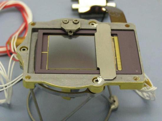
CCDs and CMOS Sensors
CCD and CMOS sensors fall into the category of focal plane array (FPA) sensors, in which multiple light sensing elements are arranged, usually into a grid, in order to gather spatial information in addition to spectral information. These sensors differ from photodiode arrays in their architecture; PDAs are comprised of multiple discrete sensors, connected through external circuitry, whereas CCD and CMOS sensors are monolithic arrays, fabricated on a single semiconductor wafer, much in the same way that modern microprocessors are produced. Additionally, CCD and CMOS sensors are integrative sensors, collecting light for an extended period of time, called an exposure, before processing the light into a signal. CCDs differ from CMOS sensors in how charge is transferred and converted into a signal, with each form offering several advantages and disadvantages.
Charge Coupled Devices (CCDs)
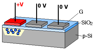
Charge coupled devices are two-dimensional arrays of metal-oxide-semiconductor structures. On a substrate of p-type silicon (or another semiconductor for more specialized applications), a thin layer of silicon dioxide is deposited to act as an insulating barrier. A grid of discrete metal contacts, or gates, is then deposited on the oxide layer, completing the basic structure, known as a pixel. Modern sensors can have as few as 4096 pixels for very small sensors, to as many as 109 pixels for very large sensors.
When the metal gates are held at a positive voltage relative to the p-type silicon, the positively charged holes in the silicon are pushed away from the gates, creating a depletion zone that acts as a potential well for any free electrons in the substrate. Each metal-oxide-semiconductor structure thus acts as a capacitor, in which charge, in the form of electrons, can be trapped and stored. Upon exposure to a light source, incident photons are absorbed by the p-type silicon substrate, generating electron-hole pairs. The electrons are drawn into the potential wells nearest to where they were generated, and are collected there in packets until the sensor is read out. This process, as illustrated in Figure 7, is accomplished by sequentially changing the potential of the metal gates along rows, moving the charge packets from gate to gate until they reach the edge of the array. Once at the edge, each individual column is quickly shifted down to the corner of the array, packet by packet, into an external circuit that measures the amount of charge contained in each packet. As the packets are localized to a specific point on the detector array, a two-dimensional image can be reconstructed from the signal, pixel by pixel; this technology forms the basis for many high-end camera sensors, including the sensors in the Hubble Space Telescope.
One of the main benefits of a CCD detector is its adaptability to a variety of different tasks. The semiconductor substrate can be changed to access alternate regions of the electromagnetic spectrum; silicon is prominent for use in the soft X-ray to near-IR region, while cadmium zinc telluride is a common material for higher energy X-rays and gamma rays, and lead sulfide is used in the lower energy IR region. Furthermore, a scintillator can be placed in front of a CCD, allowing for detection in virtually any region of the spectrum. CCDs also exhibit extremely linear spectral responses, and have very large dynamic ranges. There is however a limit to how much light a CCD can integrate, as the metal-oxide-semiconductor capacitors have upper limits to how much charge they can store. Surpassing this limit causes charge to spill over into neighboring pixels, which causes unwanted blooming around the brightest spots in images. Additionally, CCDs suffer from fairly long response times, as the charge packets under each individual gate must be moved off the grid and converted from a charge to a voltage, an operation performed by an external output amplifier. Another inherent drawback to CCDs is the read-out noise associated with moving the charge packets off the grid and processing them through an amplifier into a usable signal.
Complementary Metal-Oxide-Semiconductor (CMOS) Sensors
Complementary metal-oxide-semiconductor sensors represent a newer approach to focal plane array detectors, incorporating technology that was not fully realized when the first CCDs were developed. A detailed analysis of the architecture and circuitry of modern CMOS sensors is beyond the scope of this discussion, but the fundamental difference between CMOS sensors and CCDs can be understood through two key changes: in a CMOS sensor, the packets of charge are not moved before they are measured, and signal amplification does not occur in an external circuit. Light is collected in the same manner in both CCDs and CMOS sensors, but instead of moving these packets to an external amplifier as a CCD does, each pixel in a CMOS sensor has its own built-in operational amplifier, which provides a significant amount of signal gain on-chip as it converts the charge of a packet to a voltage. The fact that each pixel has an associated voltage allows for an alternative method of read-out that is much faster and introduces far less noise; in a process known as signal multiplexing, a common bus is sequentially connected to each pixel in a column, and the voltage is recorded. The bus is then shifted to the next column, and the process is repeated until all columns have been read. After measurement, a reset transistor built into each pixel drains the accumulated charge, and the sensor is ready to integrate another signal.
In addition to lower response times and less intrinsic noise as compared to CCDs, CMOS sensors are also much less expensive to produce, as they can be manufactured in current microprocessor fabrication facilities without any retooling. However, CMOS sensors have several disavantages; the addition of the operational amplifier and other electrical components necessary for operation blocks some of the active space on the chip, reducing the photosensitive area of each pixel. Furthermore, current manufacturing facilities are designed for microprocessors, which are by definition very small, and this places a limit on the maximum size of a CMOS sensor. In applications that call for small sensors, such as consumer-sized digital cameras, virtually all devices rely on CMOS sensors, but when larger format sensors are required, most devices utilize CCDs, which can be very large -- the primary sensor in the James Webb Space Telescope is a CCD that measures one meter across.
Other Detectors
Discussed here are several examples of photon detectors that operate in very different ways from those covered above, and are adapted for specific applications.
NMR Probes
All previously mentioned detectors require some form of electronic transition to occur in a substance; however, a great deal of spectroscopy occurs at energies far below those required for electronic excitations. One example of this is nuclear magnetic resonance spectroscopy, which measures how magnetic moments are shifted by applied electromagnetic radiation. This radiation often has frequencies on the order of several hundred megahertz, corresponding to wavelengths between 0.3 and 3 meters. None of the previously mentioned detectors are sensitive in this region, and a completely different form of detection is required. NMR probes are extremely simple in their construction: they are made from a coiled non-magnetic conductor, which acts as an antenna. An oscillating electromagnetic wave, such as a radio wave, exerts a Lorentz force on electrons within a conductor, and induces an oscillating electric current. When this process is reversed, and an electric current is applied through the coil, the probe will generate an electromagnetic wave, which can interact with a sample. In most modern NMR spectrometers, this current takes the form of a pulse, which serves to shift the bulk magnetization of a sample. When the bulk magnetization lies in the xy plane, it begins to precess about the z-axis, perpendicular to the coil. Ignoring any T2* relaxations, this precession gives rise to an oscillating magnetic field, which in turn induces an electromotive force (EMF) in the coil via the Lorentz force, manifesting as an oscillating current. This current can be directly measured, allowing for the quantization of a wide range of low-energy radiation. Operation of a probe as both a radiation source and a detector is know as quadrature detection.
The response time of the NMR coil is on the order of several hundred microseconds. This is due to the fact that the coil is a transciever; it both applies the pulse and then detects the signal. Converting from transducer to reciever takes time, as the coil will oscillate after the pulse. This is known as ringdown, and its duration is based on the amount of power sent through the coil on the pulse. If the NMR signal is detected before ringdown stops, then the resulting Fourier Transform of the spectrum will be significantly broadend by the oscillitory motion of the NMR coil. To circumvent these issues, an echo is often used. Additionanlly, the coil may be cooled to reduce thermal noise.
Thermistor Bolometers and Transition Edge Sensors
In addition to detecting photons through excitation of electrons or the induction of a current in a coil, there are several types of detector that function by measuring changes in temperature. One class of these detectors are thermistor bolometers, which exploit the fact that the resistance of a semiconductor is temperature dependent. The absorption of a photon of almost any energy will cause the temperature of the absorbing material to rise, although only slightly. However, certain semiconductors have very large changes in resistance for correspondingly small changes in temperature, allowing for the detection and quantization of small numbers of absorbed photons, in some cases as few as 10-100. In addition to being reasonably sensitive across an extroardinarily broad spectral range, thermistor bolometers are relatively inexpensive, as they are essentially made from a resistor and an ohmmeter. The primary difficulties with thermistor bolometers are response time, which requires the detector to reach thermal equilibrium after absorbing a photon, and thermal noise, which can dominate the signal at conventional temperatures. In order to get a reliable signal from a thermistor bolometer, the sensor must be kept very cold, and the temperature must be controlled with extreme precision.
An interesting subset of thermistor bolometers are transition edge sensors, or superconducting bolometers, which can reach single-photon sensitivity by taking advantage of a physical phenomenon intrinsic to superconductors. Superconducting materials are characterized by a critical temperature, below which their resistance drops to zero very suddenly. The theory behind a transition edge sensor is to measure the resistance across a superconductor held exactly at the lower edge of its critical temperature; before absorption, there is no resistance, but when even a single photon is absorbed, the temperature is raised far enough to exceed the critical temperature, and the resistance reappears and rises sharply. Transition edge sensors are some of the most sensitive detectors in existence (i.e. quantum efficiencies at or very near to 100%, with the ability to count the number of photons absorbed, even simultaneously), but the relative expense of the superconducting materials, combined with the fact that most need to be maintained at temperatures below 10 K limits their use to a small number of specialized applications.
Streak Cameras
Streak cameras are detectors designed for one purpose, and one purpose only: speed. Streak cameras allow for the observation of some of the fastest and shortest-lived processes known, with temporal resolutions down to 0.1 picoseconds. Streak cameras make this possible through the conversion of a time-resolved signal into space-resolved data. A stream of photons is absorbed by a conventional photocathode, ejecting photoelectrons into a cathode ray tube, where they are accelerated towards a CCD detector by an electric field. During this acceleration, however, the electrons pass through an electric field perpendicular to the direction they are moving. A set of plates on either side of the cathode ray tube are held at a potential that causes the electrons in the tube to deflect sideways. By applying a time-varying potential difference across the plates, the electrons experience a time-dependent deflection, causing them to form a streak moving from one side of the CCD to the other. In this way, the time at which a photon was absorbed, and a photoelectron emitted, is directly related to the lateral position of the signal on the CCD detector. As the potential difference between the plates can be varied extremely quickly, and CCD detectors can be made relatively large, astonishing time resolution is possible. It has been demonstrated that streak cameras can directly observe and track a laser pulse propagating through air.
References
- Barbarino, G.; Asmundis, R.; De Rosa, G.; Fiorillo, G.; Gallo, V.; Russo, S. A new high-gain vacuum photomultiplier based upon the amplification of a Geiger-mode p-n junction. Nucl. Instrum. Meth. A. 2008, 594, 326–331. DOI: 10.1016/j.nima.2008.06.026.
- Eisaman, M. D.; Fan, J.; Migdall, A.; Polyakov, S. V. Single-photon sources and detectors. Rev. Sci. Instrum. 2011, 82, 071101. DOI: 10.1063/1.3610677.
- Grossman, W. E. L. A comparison of optical detectors for the visible and ultraviolet. J. Chem. Ed. 1989, 66, 697-700.
- Hungerford, G.; Birch, D. J. S. Single-photon timing detectors for fluorescence lifetime spectroscopy. Meas. Sci. Technol. 1996, 7, 121-135. DOI: 10.1088/0957-0233/7/2/002.
- Irwin, K. D.; Hilton, G. C. Transition edge sensors. Top. Appl. Phys. 2005, 99, 63-149.
- Jach, T.; Ullom, J. N.; Elam, W. T. The microcalorimeter X-ray detector: A true paradigm shift in X-ray spectroscopy. Eur. Phys. J. Spec. Top. 2009, 169, 237-242. DOI: 10.1140/epjst/e2009-00998-3.
- Renker, D.; Lorenz, E. Advances in solid state photon detectors. J. Instrum. 2009, 4, P04004. DOI: 10.1088/1748-0221/4/04/P04004.
- Rogalski, A. Progress in focal plane array technologies. Prog. Quant. Electron. 2012, 36, 342-473. DOI: 10.1016/j.pquantelec.2012.07.001.
- Townsend, P. D. Photocathodes—past performance and future potential. Contemp. Phys. 2003, 44, 17-34. DOI: 10.1080/00107510302717.
Problems
- What physical phenomenon is the basis for photocathode detectors, and how is this different from solid-state semiconductor detectors?
- How does dynamic range differ from the range of spectral response?
- Of the types of noise discussed, which can be lessened by lowering the temperature of the detector, and why?
- What is one advantage and one disadvantage of a CCD over a CMOS sensor?
- What allows a streak camera to attain such mind-boggling temporal resolution?
Answers
- The photoelectric effect, or the ejection of an electron from the surface of a conductor upon absorption of a photon, is the basis for photocathode detectors. Solid-state semiconductor detectors are based on the generation of electron-hole within a solid semiconductor; the excited electrons are not ejected from the material.
- A spectral response range is the variety of photon energies (varying wavelength, constant photon flux) to which the detector is sensitive, whereas a dynamic range is the variety of photon intensities (varying photon flux, constant wavelength) for which the detector can generate a reliable signal.
- Thermal noise and dark current noise are temperature-dependent, and can be reduced by cooling the detector. For each type of noise, the speed of random charge migration or generation of thermionic electrons or electron-hole pairs is possible due to the distribution of thermal energy in the detector; if the thermal energy is lessened, both the speed of charge carriers and the statistical probability of an electronic excitation are reduced, lowering the overall thermal noise.
- One advantage of a CCD over a CMOS sensor is the ability to create very large pixel arrays, capable of extremely high resolutions. One disadvantage is that CCD detectors are invariably more expensive than comparable CMOS sensors.
- The conversion of time-domain data into spatial data allows for the relative expansion of the dataset onto a larger frame of reference. For example, if an electron beam is swept across a 1,000 pixel CCD in one nanosecond, then the time difference between individual pixels corresponds to one picosecond.
Contributors
- Josh Greenfield, UC Davis