
Semiconductor and Solid-state lasers
- Page ID
- 67374
\( \newcommand{\vecs}[1]{\overset { \scriptstyle \rightharpoonup} {\mathbf{#1}} } \)
\( \newcommand{\vecd}[1]{\overset{-\!-\!\rightharpoonup}{\vphantom{a}\smash {#1}}} \)
\( \newcommand{\dsum}{\displaystyle\sum\limits} \)
\( \newcommand{\dint}{\displaystyle\int\limits} \)
\( \newcommand{\dlim}{\displaystyle\lim\limits} \)
\( \newcommand{\id}{\mathrm{id}}\) \( \newcommand{\Span}{\mathrm{span}}\)
( \newcommand{\kernel}{\mathrm{null}\,}\) \( \newcommand{\range}{\mathrm{range}\,}\)
\( \newcommand{\RealPart}{\mathrm{Re}}\) \( \newcommand{\ImaginaryPart}{\mathrm{Im}}\)
\( \newcommand{\Argument}{\mathrm{Arg}}\) \( \newcommand{\norm}[1]{\| #1 \|}\)
\( \newcommand{\inner}[2]{\langle #1, #2 \rangle}\)
\( \newcommand{\Span}{\mathrm{span}}\)
\( \newcommand{\id}{\mathrm{id}}\)
\( \newcommand{\Span}{\mathrm{span}}\)
\( \newcommand{\kernel}{\mathrm{null}\,}\)
\( \newcommand{\range}{\mathrm{range}\,}\)
\( \newcommand{\RealPart}{\mathrm{Re}}\)
\( \newcommand{\ImaginaryPart}{\mathrm{Im}}\)
\( \newcommand{\Argument}{\mathrm{Arg}}\)
\( \newcommand{\norm}[1]{\| #1 \|}\)
\( \newcommand{\inner}[2]{\langle #1, #2 \rangle}\)
\( \newcommand{\Span}{\mathrm{span}}\) \( \newcommand{\AA}{\unicode[.8,0]{x212B}}\)
\( \newcommand{\vectorA}[1]{\vec{#1}} % arrow\)
\( \newcommand{\vectorAt}[1]{\vec{\text{#1}}} % arrow\)
\( \newcommand{\vectorB}[1]{\overset { \scriptstyle \rightharpoonup} {\mathbf{#1}} } \)
\( \newcommand{\vectorC}[1]{\textbf{#1}} \)
\( \newcommand{\vectorD}[1]{\overrightarrow{#1}} \)
\( \newcommand{\vectorDt}[1]{\overrightarrow{\text{#1}}} \)
\( \newcommand{\vectE}[1]{\overset{-\!-\!\rightharpoonup}{\vphantom{a}\smash{\mathbf {#1}}}} \)
\( \newcommand{\vecs}[1]{\overset { \scriptstyle \rightharpoonup} {\mathbf{#1}} } \)
\(\newcommand{\longvect}{\overrightarrow}\)
\( \newcommand{\vecd}[1]{\overset{-\!-\!\rightharpoonup}{\vphantom{a}\smash {#1}}} \)
\(\newcommand{\avec}{\mathbf a}\) \(\newcommand{\bvec}{\mathbf b}\) \(\newcommand{\cvec}{\mathbf c}\) \(\newcommand{\dvec}{\mathbf d}\) \(\newcommand{\dtil}{\widetilde{\mathbf d}}\) \(\newcommand{\evec}{\mathbf e}\) \(\newcommand{\fvec}{\mathbf f}\) \(\newcommand{\nvec}{\mathbf n}\) \(\newcommand{\pvec}{\mathbf p}\) \(\newcommand{\qvec}{\mathbf q}\) \(\newcommand{\svec}{\mathbf s}\) \(\newcommand{\tvec}{\mathbf t}\) \(\newcommand{\uvec}{\mathbf u}\) \(\newcommand{\vvec}{\mathbf v}\) \(\newcommand{\wvec}{\mathbf w}\) \(\newcommand{\xvec}{\mathbf x}\) \(\newcommand{\yvec}{\mathbf y}\) \(\newcommand{\zvec}{\mathbf z}\) \(\newcommand{\rvec}{\mathbf r}\) \(\newcommand{\mvec}{\mathbf m}\) \(\newcommand{\zerovec}{\mathbf 0}\) \(\newcommand{\onevec}{\mathbf 1}\) \(\newcommand{\real}{\mathbb R}\) \(\newcommand{\twovec}[2]{\left[\begin{array}{r}#1 \\ #2 \end{array}\right]}\) \(\newcommand{\ctwovec}[2]{\left[\begin{array}{c}#1 \\ #2 \end{array}\right]}\) \(\newcommand{\threevec}[3]{\left[\begin{array}{r}#1 \\ #2 \\ #3 \end{array}\right]}\) \(\newcommand{\cthreevec}[3]{\left[\begin{array}{c}#1 \\ #2 \\ #3 \end{array}\right]}\) \(\newcommand{\fourvec}[4]{\left[\begin{array}{r}#1 \\ #2 \\ #3 \\ #4 \end{array}\right]}\) \(\newcommand{\cfourvec}[4]{\left[\begin{array}{c}#1 \\ #2 \\ #3 \\ #4 \end{array}\right]}\) \(\newcommand{\fivevec}[5]{\left[\begin{array}{r}#1 \\ #2 \\ #3 \\ #4 \\ #5 \\ \end{array}\right]}\) \(\newcommand{\cfivevec}[5]{\left[\begin{array}{c}#1 \\ #2 \\ #3 \\ #4 \\ #5 \\ \end{array}\right]}\) \(\newcommand{\mattwo}[4]{\left[\begin{array}{rr}#1 \amp #2 \\ #3 \amp #4 \\ \end{array}\right]}\) \(\newcommand{\laspan}[1]{\text{Span}\{#1\}}\) \(\newcommand{\bcal}{\cal B}\) \(\newcommand{\ccal}{\cal C}\) \(\newcommand{\scal}{\cal S}\) \(\newcommand{\wcal}{\cal W}\) \(\newcommand{\ecal}{\cal E}\) \(\newcommand{\coords}[2]{\left\{#1\right\}_{#2}}\) \(\newcommand{\gray}[1]{\color{gray}{#1}}\) \(\newcommand{\lgray}[1]{\color{lightgray}{#1}}\) \(\newcommand{\rank}{\operatorname{rank}}\) \(\newcommand{\row}{\text{Row}}\) \(\newcommand{\col}{\text{Col}}\) \(\renewcommand{\row}{\text{Row}}\) \(\newcommand{\nul}{\text{Nul}}\) \(\newcommand{\var}{\text{Var}}\) \(\newcommand{\corr}{\text{corr}}\) \(\newcommand{\len}[1]{\left|#1\right|}\) \(\newcommand{\bbar}{\overline{\bvec}}\) \(\newcommand{\bhat}{\widehat{\bvec}}\) \(\newcommand{\bperp}{\bvec^\perp}\) \(\newcommand{\xhat}{\widehat{\xvec}}\) \(\newcommand{\vhat}{\widehat{\vvec}}\) \(\newcommand{\uhat}{\widehat{\uvec}}\) \(\newcommand{\what}{\widehat{\wvec}}\) \(\newcommand{\Sighat}{\widehat{\Sigma}}\) \(\newcommand{\lt}{<}\) \(\newcommand{\gt}{>}\) \(\newcommand{\amp}{&}\) \(\definecolor{fillinmathshade}{gray}{0.9}\)In both solid-state and semiconductor lasers the lasing medium is a solid. Aside from this similarity, however, these two laser types are very different from each other. In the case of the solid-state lasers the lasing species is typically an impurity that resides in a solid host, a crystal of some sort. The crystal modifies some of the quantized energy levels of the impurity, but still the lasing is almost atomic - similar to gas lasers. The physics of the quantization, in the case of semiconductor lasers, is very different. In addition, solid-state lasers are always optically pumped, whereas semiconductor lasers are excited by the passage of electric current through them.
We have already seen how atomic energy levels become modified when two or more atoms bind to form a molecule. The energy quantization picture becomes more complex when atoms bind together to form a solid. Below, we will first examine energy quantization in solids before we begin a more detailed examination of solid-state and semiconductor lasers.
Crystals and Energy Bands
You may recall from high school chemistry that a model that is very successful in explaining the electronic composition of stable atomic species is called the shell model. In this model, very similar to the planetary model, the atom is thought to be made of shells of different types. Each shell-type can accommodate a certain number of electrons. For example, an "s-shell" can be occupied by no more than two electrons, whereas p-shells can have up to six electrons in them, etc. To "make stable atoms" we start by filling electrons in these shells starting in "level" 1, then level-2, etc., following the specified hierarchy: 1s; 2s, 2p; 3s, 3p; 4s, 3d, 4p; 5s, 4d, 5p; etc. (Remember that the chemistry of materials is due to electromagnetic interactions alone, so for this we only need to concern ourselves with electrons.) We start with the innermost shell, an s-shell. Our first atom-type has one electron in its s-shell; that's of course the hydrogen atom, H. The next atom has two electrons in its s-shell; that's He. The third atom on our list (see the Periodic Table) has three electrons, two in its 1 s-shell and then one in its 2 s-shell; and so on. According to this model, which incidentally is very well supported by the more rigorous and fundamental laws of Quantum Mechanics, atoms prefer to fill their outer most shell. Inert gases, for example, all (except for He) have a completely filled outer p-shell. Those atoms that manage this are energetically very stable. Those that don't would then prefer to interact with another atom of the correct type to allow an exchange of electrons so that they come closer to fulfilling this desire for closed shells in order to reduce their overall energy. A bond between two types of atoms by this give-and-take is strongest when both atoms get the most fulfillment - both end up with closed shells.
A good example of this is the case of table-salt: NaCl. Sodium atoms, Na, are hydrogenic (hydrogen-like); i.e. they have one electron in their outermost shell, which is an s-shell just outside an inert gas shell. So, to emulate the rare gases, all they need to do is to get rid of this electron. They cannot do this on their own (why?), but they can bind with an atom that wants an additional electron to complete its outer most shell. This happens to be true for the chlorine atom that has 5 electrons in its outermost shell, a p-shell. By sharing this electron with chlorine, the sodium atom still remains neutral, but now it, as well as the Cl, both end up with "filled" outer shells. In more ways than one, this is a happy marriage. Of course, in a grain of salt there are many Na and Cl atoms. (One grain of salt has roughly about 1 mg of mass. One proton is about 10-27 kg. How many atoms are then in one grain?) These atoms arrange themselves in a very organized pattern, called a crystal. These are rows and columns of atoms, as in a three-dimensional array, with interchanging Na and Cl species. In a salt crystal, a Na atom shares its electron with several Cl atoms, and yet because of the geometry of the crystal each Cl atom ends up with a net total of one extra and each Na atom with only one fewer electron (how?).
The electric attraction of the electrons to the atom's positively charged nucleus is the primary force that holds the atom together as a whole. So, in our shell model of the atom we must also account for the difference in attraction of electrons in different shells as well as the repulsion among the electrons themselves. Electrons in outer shells are further away from the nucleus, so their force of attraction is weaker than the inner shell electrons. In this respect, those electrons that belong to the unfilled outermost shell are the most loosely bound electrons in the atom. These electrons are the ones that are mostly responsible for the atom's interaction with another atom, so they are given a special name: the valence electrons.
How is the shell model related to our picture of atomic energy levels? It is primarily the valence electrons that connect these two pictures. Each atom species has its own unique energy levels, but its shell structure is not unique. When it is in its ground state, then its shells are filled according to the shell model's recipe, mentioned above. But once the atom is excited, then its electron configuration will change. The first excited state, for example, could require the valence electron to jump into the next higher shell. Further excitation of the atom could lead to even more drastic changes in its shell structure. But each of the excited energy levels corresponds to a different occupation of the accessible shells by the atom's electrons.
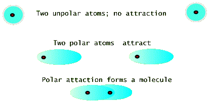
If atoms were made of (stationary) electrostatic charges, then most atomic species would have no reason to get together to make molecules or solids. But fortunately for us, this is not the case. Two neutral atoms can attract each other simply by changing their charge distribution so that they each become polar, i.e. the electron cloud of charges shifts over so that its center is not at the positive nucleus (see the figure below). In this sense even atoms of the same species find it energetically favorable to form a molecule. Because of this two totally neutral atoms of nitrogen prefer to form an N2 molecule even in the gas form. See the model drawing, below, which shows three time frames. The top frame shows two atoms with spherically symmetric charge distributions. These atoms do not initially interact with each other. But a momentary polarization of one atom can cause the other atom to polarize as well. This is the picture in the middle frame. The bottom frame the shows that two polarized atoms attract and form a molecule in which the electronic clouds of the two atoms overlaps.
When we cool a gas, the ease with which it makes a liquid has a great deal to do with how easily the atoms in the gas form a molecule. Things get even more interesting when the liquid is further cooled to make a solid. The form, i.e. atomic structure, in the solid has not only to do with the atoms wanting to share electrons, but also with a totally different aspect of energy for a large collection of atoms. This relates to the probability of arrangements, or the so called entropy. What concerns us here is that for some species of atoms the lowest possible energy is reached when the atoms arrange themselves is a very regular and repeatable array of positions, called a crystal.
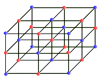
In every-day terminology the word "crystal" usually refers to a glassy and transparent object. But in our sense of the "regular network" a crystal may be totally opaque. In fact, most metals are crystalline in structure and are not at all transparent (at least in the visible range). Why should atoms form a regular array and make up a crystal? Why shouldn't they just clump together? In most substances atoms clump randomly, forming a solid. But in some special situations atoms crystallize to make very regular network structures. These networks can have different geometrical regularities. For example, in some crystals, the network structure is a simple cube that repeats in all directions. One atom sits at each corner of the cube, making up a simple cubic crystal. In a variation of this, in addition to the simple cubic structure each face of the cube has an atom at its center; this is called a face centered cubic crystal, etc. The salt crystal of NaCl has the simple cubic structure in which Cl and Na atoms occupy alternate corners of the cube, shown below:
This network structure in the crystal is called a lattice. The atoms in the lattice are not motionless. They jiggle and oscillate, but on average remain at a fixed site. The higher the temperature of the solid, the more vigorous is the jiggling oscillation of the lattice atoms. In the case of metals, which are electric conductors, the electron clouds of the lattice atoms overlap allowing the valence electrons to jump from lattice site to site when an electric potential (or voltage) is applied to the metal. So conductors allow these electrons to move freely - they are called "free electrons" - and make up an electric current, or flow of electric charge. Insulators, on the other hand, do not share their electrons and they are not free to migrate around. These materials, such as glass, wood, rubber, most plastic, and pure water, do not support electric currents under normal circumstances. What happens to the quantized energy levels of an atom when it is influenced by the presence of all the other lattice atoms in the crystal? It turns out that the idea of quantized energy levels still remains valid, but in a totally different picture. Instead of each atom having its own set of energy levels the solid as a whole can be described by a set of so called energy bands. In this picture the bands represent the quantized energy of the whole crystal. This is represented by the number of the energy bands, their energy widths, the gap between the bands, and whether the band is full, partially full, or empty. So, in a way these bands in the crystal play a similar role to the shells in the case of individual atoms. Just as in the atomic shell model we "fill" energy bands in a solid with electrons. Depending on the atomic species that make up the crystal, these bands get filled or not. For example, in the case of the sodium atom that we examined above, the corresponding energy band picture for its solid form is shown below:
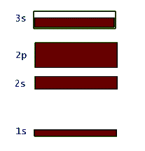
Again it should be stressed that this band picture is really a combination of the energy-level-diagram and the occupancy picture of the shell model. So, here the large gap between the 1s and 2s bands represents the relatively large amount of energy that is necessary to promote an electron in a single atom of sodium from the 1s to the 2s shell. Also the filled 1s, 2s, and 2p bands indicate Na's shell structure. At the same time, the unfilled 3s band shows that these valence electrons in solid sodium can continuously change their energy within this band. This is totally due to the huge number of atoms in the solid structure and was not allowed in the quantized single atom.
Insulators, Semiconductors, and Conductors
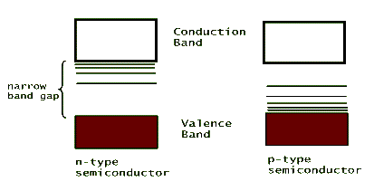
The electric conductivity of different materials is a consequence of their individual band structure. Metals, such as sodium, copper, aluminum, etc. have a crystalline band structure in which the upper most energy band, the valence band, is partially filled (or better yet, partially empty!). Electrons in this band can gain energy from an applied external electric potential, such as a battery, without the restriction of quantization. Insulators, on the other hand, have full valence bands, so for an electron to be promoted to its next higher available energy it has to leave this band and jump into the upper empty band. This is possible, but it takes a huge electric potential to make it happen (that's why lightning can pass through walls and kill people, but typical wiring is safe with just a thin plastic insulation over it). Semiconductors are intermediate between insulators and conductors. Their band structure is the same as an insulators' but the separating gap between their valance band and the next empty band, the conduction band, is very narrow.

Because of this narrow so called band gap, semiconductors can use the thermal energy of their lattice (collisions between the valence electrons and the oscillating lattice atoms) to promote a few of their valence electrons to the conduction band. In this way these material can conduct electricity, but because of the limited number of electrons that get promoted, they are not very good conductors. Examples of crystalline materials with narrow band gaps are silicon (Si) and germanium (Ge). In both of these materials the outermost shell is a partially filled p-shell with only two (out of a maximum of 6) electrons in it. In these crystals the two valence p-shell electrons are shared by the other neighboring atoms in the lattice.
To make a better conductor out of these semiconductors, atom impurities are introduced in the crystal formation through a process called doping. If one of the silicon atoms in the lattice is replaced by an arsenic (As) atom, which has three p-shell valence electrons, then the extra electron becomes loosely attached to its mother atom. This loose electron can take part in the electric conduction and therefore increases the conductivity of the crystal. Strangely enough, a similar process can occur if one of the silicon atoms is replaced by a gallium (Ga) atom, which has only one p-shell valence electron. In this case, the Ga impurity strongly attracts one of the p-shell electrons from one of its Si neighbors. This leads to the production of a so called "electron hole". The resulting electron vacancy (hole) can travel in the crystal just as an electron would - but in the opposite direction - and results in an increased conductivity. Doped Si crystals with extra electrons, negative carriers, are referred to as n-type; those with holes are called p-type. These impurities modify the crystals' energy band structure by introducing atomic-type energy levels between the valance and conduction bands of the crystal and thus further reduce the band gap. This is shown below:
Semiconductor Devices
Diodes are the most basic of semiconductor devices. They are simply one-way conductors. By suitably doping a Si crystal, its conductivity can be altered to make it behave as a conductor in one direction and an insulator in the other direction! This is commonly done in a p-n junction. When the crystal is being formed it is first introduced to a donor-type impurity (say As for an Si crystal). As the crystal grows the concentration of the donar impurity is reduced and replaced with a growing concentration of an acceptor impurity (say Ga for an Si crystal). So, the resulting crystal begins at one end as an n-type and eventually becomes a p-type at the other end. The n-type portion has a large concentration of electrons and the p-type end a large concentration of holes. This variation causes this device to act as an effective insulator for the flow of electricity in it from the n to the p-side, but a very good conductor in the opposite direction. So, unlike a regular conductor that allows internal flow of electricity in both directions, this device acts like a unidirectional valve. An electronic component that allows electricity to flow in one way (the forward bias), but not the opposite way (reverse bias) is called a diode.
Transistors are the most common of semiconductor devices. They are controllable switches made from either p-n-p or n-p-n arrays of doped silicon. Today's technology can put millions of transistors together into single integrated modules, or chips, to make a large variety of different types of devices such as computer memory chips or microprocessors.
Another semiconductor device is the familiar solar cell. This is also a p-n junction with variations in the hole and electron concentrations along the crystal. When light strikes this device it excites bound electrons from the valence band into the conduction band. This creates not only a mobile electron, but a hole in the valence band. Both the electron and the oppositely traveling hole produce electric current. So, when light strikes this device it behaves as a source of electricity, just like a battery. In the case of a battery chemical energy is used to produce free electrons and thereby the electric current. In solar cells photon energy is converted into the production of electron-hole pairs and the resulting electric current in the junction.
Light Emitting Diodes (LEDs) behave just the opposite of solar cells. In these devices, also having a p-n junction, the combination of hole-electron pairs, created by an applied source of electricity, give off light. So, light is produced when a free electron fills a hole, i.e. a vacancy, in the crystal that is created by the presence of a p-type impurity. The light generated by LEDs is very broad-band and not of a single wavelength. It is also generated in all directions, so these devices do not make laser light. But they are useful light sources in that they are very compact and consume little electric power. To make them more efficient and reduce absorption of the generated light by the crystal's lattice, typically the junction is made near the surface. These light sources were first made in the early 1960's. Their creation soon lead to the discovery of semiconductor lasers.
Semiconductor Lasers
Also known as diode-lasers, these are by far the most inexpensive and commonly used lasers in the world. The first diode-laser was invented in 1962 at the General Electric Research and Development Center, in Niskayuna, New York - just a few miles from the Union College campus. But it was not until the early 1980's, with the development of innovative semiconductor chip manufacturing techniques, that their mass production reached the consumer market. Similar to their LED cousins, these semiconductor devices generate light from the energy extracted when electron-hole pairs recombine. Also, as in the case of LEDs, the electron-hole pairs in the semiconductor lasers are produced by the flow of electric current in the junction - this is called the injection current. The primary difference between these lasers and photodiodes is that at high injection currents the electron-hole pair densities increase to produce population inversion, which leads to lasing. These lasers, in fact, behave very much like LEDs until the critical injection current, called the threshold current, is reached.
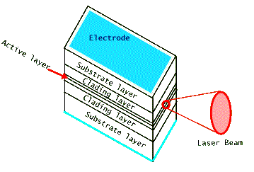
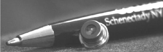
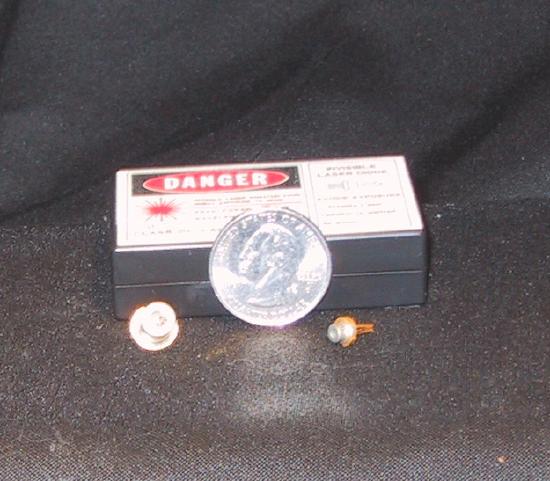
A typical semiconductor laser, shown above, is about a few hundred microns in dimension, much smaller than a grain of table salt. (Recall that a human hair is about 100 microns thick.) It produces light from an active area which is still smaller, a few tenths of one micron, perpendicular to the flow of electric current. Therefore (recall that diffraction from a very small exit aperture leads to a large angular spread of the beam) its laser light is very divergent and requires the use of a lens to collimate it. Most commonly used diode lasers are made of several different layers of compound semiconductors, often GaAlAs. Both the doping and thickness designs of these layers are used to control the confinement of laser light in the active lasing region. For some applications reflective coatings are deposited on the front and back facets to increase the efficiency of the optical amplification by acting as mirrors. But in most cases simple cleaving of the output facets leads to sufficient light amplification for lasing action. One of the drawbacks of the diode laser's small size is that it has a short coherence length. This limits its use in applications that require large coherence lengths, such as interferometry and holography. But the portability of its size makes it far more useful in many other applications. Below are two photographs of typical diode laser modules, shown in comparison with a typical writing pen or with a quarter. Notice that the laser's packaging "can" has a glass window to protect the fragile diode laser housed inside it. This package also includes a diagnostic photodiode detector that measures the output laser light leaking from the back facet of the laser chip.
Diode lasers operate in several modes. Their wavelength depends primarily on the size of the band gap of the semiconductor. But the design of the semiconductor layers, as well as active feedback into the laser can generate band-widths of a few hundred kHz. Since changing the temperature of the diode expands or contracts the crystal and in this way changes the dimensions of the laser's optical cavity, the laser's wavelength can be changed either by adjusting the injection current or by directly changing diode's temperature with another device. Wavelength tunability of a typical diode laser is about a few nm over a temperature range of about 10 oC. (This is very small compared to tunable dye lasers, for example.) Room temperature diode lasers have been manufactured with wavelength outputs from a few microns in the IR all the way to the green in the visible. Researchers are currently producing blue diode lasers, but these are not yet mass produced.
These lasers have a very high efficiency and are manufactured to produce laser light from a few mW to several tenths of a Watt. They can be made to operate in cw as well as in a pulsed mode. Because of their compact size an array of these can be manufactured on single chips, called laser diode arrays, that can generate output powers in the Watt range. But the single property that makes these lasers extremely useful is that their output light can be modulated at very fast rates. Because of this, and the very narrow band-width light that they can produce, diode lasers have overtaken all other lasers used in the communication industry.
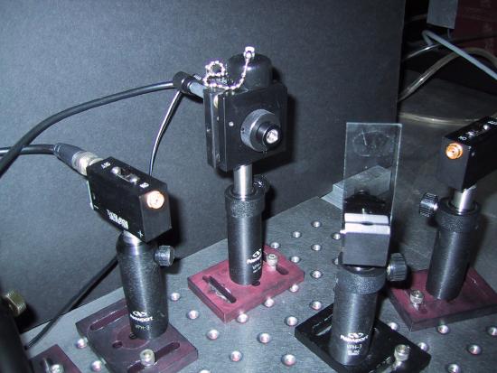
Measurement of the speed of light using a GHz pulsed diode laser (center) with its beam split by the glass slide to either directly enter the fast photodiode detector on the right or to travel several meters distance before being steered to enter the second photodiode detector on the left. By measuring the total path traveled and the time between the arrival of the two pulses, the speed of light can be measured on a table top to better than 1% accuracy.
Solid-state Lasers
The first laser ever made, the ruby laser, was a solid-state laser. In this laser the lasing is a result of atomic transitions of an impurity atom in a crystalline host. Even though the atomic levels of the lasing species are often modified because of the host crystal, the lasing process is atomic and very different from that in semiconductor lasers. All solid-state lasers are pumped optically. So, in these lasers the host must be transparent to the pumping radiation. (Why?) Also, the host must be a good heat conductor in order for it to effectively dissipate waste energy that is not used for lasing. Below we will review two of the most commonly used solid-state lasers: the ruby and YAG lasers.
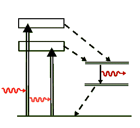
Ruby is an aluminum oxide (\(Al_2O_3\)) crystal, called sapphire, with a small amount of chromium oxide (\(Cr_2O_3\)) added to it. Sapphire is colorless and transparent, but the chromium doped crystal is pinkish-red in color because it strongly absorbs both in the green and in the blue. When this crystal is excited through the absorption of blue and/or green light it soon causes excitation of a meta-stable energy state of the chromium ion (\(Cr^{3+}\)). After a typical lifetime of a few milliseconds this state de-excites to the ground state with the emission of a 694.3 nm photon, which is visibly red in color. So, the primary role of the aluminum oxide crystal, aside from hosting the chromium ion, is to absorb the pump energy and to excite the ion through collisions.
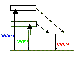
The above simplified energy-level diagram shows the two optically pumped broad levels that quickly decay into the upper metastable lasing levels via non-radiative transitions (shown with dashed arrows). The energy of these non-radiative transitions is lost to the crystal as heat. Finally, the chromium ion de-excites back to its ground state by emitting the laser's 694.3 nm photon. Note that Ruby is a 3-level laser and as such it requires a good deal of pump energy to achieve a population inversion. It can not produce a cw beam but produces a series of bright laser pulses.
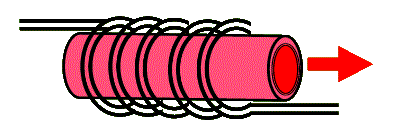
To achieve population inversion, a strong pulse of broadband light is used to excite most chromium ions to their excited state. This is typically accomplished with the use of a helical flashlamp that surrounds a cylindrical ruby crystal. The two ends of this cylinder are coated (using evaporation techniques) to reflect the red 694.3 nm light. Because the wavelength output of the ruby laser is narrow-band and the pulse of light can be strong, this laser is one of the most preferred for holography. The following diagram shows a ruby rod surrounded with a helical flashtube. The cylindrical ends are coated for reflectivity in the red to form the optical cavity of the laser.
Typical ruby rods range in length from about 10 cm to 1/4 m and in diameter from a few to about 25 mm. The standard ruby lasers produce a few ms long duration pulses that range in energy from 10 to 100 J. But because ruby rods degrade quickly from excessive heating, these lasers are often operated at rather slow repetition rates (rep-rate) of few pulses per second (few Hz).
Applications that require large numbers of photons in a short period of time, benefit from laser pulses that are short in duration, but have a high peak. The following graph shows two pulses of light that carry equal number of photons (equal areas under their graphs), but have very different peak heights.
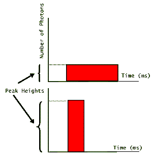
The one that has the higher peak, then has the shortest duration. (Note that for simplicity these pulses are depicted as rectangular in shape suggesting that lasing turns on and off at precise instants. In reality, however, laser pulses look more like hills; gradually increasing, reaching a peak, and then gradually decreasing before fully turning off.) Since the energy of each photon is fixed depending on the value of its wavelength (or its frequency), then both of these pulses carry the same amount of energy. For example, if we are told that the above pulses each have N photons emitted by a ruby laser, then we could easily calculate the pulse energies:
\[\text{pulse energy} = \text{(number of photons in the pulse)} \times \text{(energy of a single photon)} \nonumber \]
i.e. pulse energy = N x (hn) = N x ( hc / l ) = N x { (6.63 x 10⁻³⁴) (3.00 x 10⁸) / (694.3 x 10⁻⁹) }
\[ = N \times ( 2.87 \times 10^{-19}) Joules. \nonumber \]
Alternatively, if we were told that each of the above ruby laser pulses is a 10 J pulse, then we could easily calculate the number of photons in each pulse:
number of photons = N = (pulse energy ) / (energy of a single photon)
or,
\[N = \dfrac{10}{ 2.87 \times 10^{-19}} = 3.5 \times 10^{19} \nonumber \]
Devices that measure laser light energies do not count the number of photons. Instead, they measure the energy that the photons produce in the device. (For example, photodiodes, which work like solar cells, absorb the photon energy and create electron-hole pairs, which produce a voltage across the p-n junction. This voltage is proportional to the absorbed energy and is displayed by the device indicating the pulse energy.) The following graphs are more realistic depictions of pulse energy measurements:
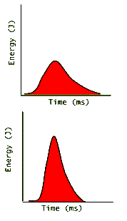
Here again we see two graphs of roughly equal areas and therefore equal pulse energies. The top pulse creates "less energy for a longer time" while the lower one creates "more energy for a shorter time". Since power is defined as:
power = ( energy ) / ( time ) (with units of 1 Watt = 1 Joule / 1 second )
Then the pulse shown on the lower graph has much more power than the top one. (Why?) This is called the pulse power, or the peak power. For comparison with a cw laser it is convenient to average the energy of the pulse over not just its duration, but also over the time that the laser is on but there is not light emitted from it. To do this, all we need do is divide the total pulse energy by the time interval from when a pulse begins until the time that the next pulse begins; i.e. the "pulse-to-pulse time":
average power = ( pulse energy ) / ( pulse-to-pulse time )
In pulsed lasers there are several ways to achieve a large peak power. One of these is called Q-switching, which refers to an increase in the efficiency of the optical cavity. The Q of an amplifier is just a measure of its efficiency. An amplifier that uses little energy for its amplification is said to have a large-Q. In pulsed lasers a method of increasing efficiency is to simply increase peak power. This can happen when instead of producing a long pulse one makes the laser produce a shorter pulse with a larger peak energy. One method for doing this is, instead of causing stimulated emission, to let the medium buildup more and more of a population inversion in its metastable state. This can be done rather easily by "blocking" one of the optical cavity's reflective mirrors for long enough that the maximum number of the atoms are in the upper laser level. Then to cause all of the atoms in the upper lasing level to undergo stimulated emission "all at once" a very quick "unblocking" of the reflective mirror results in many atoms to undergo stimulated emission simultaneously; therefore the resulting laser pulse has a high peak power. In this way Q-switched lasers can produce very high peak powers, in the hundreds of megawatts!
YAG Lasers
Yttrium-Aluminum-Garnet (\(Y_3Al_5O_{12}\)), YAG, is a clear and transparent crystal that is most commonly used as the host crystal for neodymium impurity atoms in Nd:YAG lasers. Even though the lasing transition occurs in the Neodymium (Nd) ions, these lasers are often called YAG lasers. Typically 1 - 2% of the Y is replaced by Nd in these lasers. Similar to the ruby laser, here again the crystal not only hosts the atom, but also its broad absorption bands (in the presence of the Nd-impurity) effectively absorb optical radiation - mostly around 700 nm and 800 nm. This energy is then transferred to the impurity ions through non-radiative processes.
Similar to the level diagram for the ruby laser, the above diagram is a simplified representation of the transitions for the neodymium ion, Nd+++, that take place in the YAG laser. Again, the dashed arrows indicate non-radiative transitions, where the energy lost in them is transferred as heat to the crystal. But unlike the ruby laser, the Nd:YAG is a four-level laser and has much more efficient lasing transitions than the ruby laser. Because of this efficiency in population inversion it can be pumped to produce a wide variety of laser output energies and can be operated in the cw as well as pulsed modes. The lasing photon has a wavelength of 1064 nm, well in the IR range.
Another host used for Nd is plain glass, but its optical and thermal properties are not as desirable as YAG's. The trade off is that growing large YAG crystals is not easy. A typical YAG rod, which is drilled out of a crystal block, is smaller than 1 cm in diameter and from a few to 10 cm in length. Still, these lasers can produce high output powers by using several rods in tandem. Pulsed YAG lasers can produce high peak powers by Q-switching and/or by using several rods as amplifiers. When used as amplifiers, the rods are not coated for reflectivity to produce optical amplification in the rod. Instead, the output of the first rod (the oscillator) is used as a Q-switch to generate stimulated emission in the next rod (the amplifier), and so on.
In the cw mode YAG lasers are pumped either by an arc lamp or a semiconductor laser. Pumping with a diode laser is more efficient because the diode's wavelength can be chosen to closely match the absorption of the YAG. Flashlamps are often used for pulsed operation of these lasers. In this mode Q-switching the laser can produce ns pulses with relatively high peak powers. But, to reach very high powers, like that generated by the NOVA laser, many rod amplifications are necessary.
YAG lasers are extremely versatile. They are used in applications from welding and drilling to range finding. Because their output wavelength is not visible, YAG lasers are used in many applications that require secrecy; from military to security applications. It is now possible to convert IR radiation into the visible range using so called non-linear crystals (also known as second-harmonic-generators). When high density photons impinge on such a crystal, the non-linear properties of its index of refraction causes the crystal to absorb two long wavelength photons and generate, in their place, one photon with twice their energy and therefore half their wavelength. Using these crystals, the YAG laser wavelength can be shortened to 532 nm (1064 nm/2), which is seen by the eye as green light. Today's green-colored laser pointers are diode-pumped YAG lasers with doubling crystals.
Although we can change the wavelength of the YAG laser from IR to green (and even further into UV, via another second harmonic generation), this is not a continuous tuning. Other interesting solid-state lasers, called vibronic lasers, use effective bands as their lower lasing level. In this way these lasers can produce a tunable output; i.e. one with a continually changeable wavelength. The most commonly used laser of this type is the Ti:sapphire laser, which is an aluminum oxide crystal, the same as ruby's host, but doped with titanium instead of chromium atoms.
Questions on Semiconductor & Solid-state lasers
- What does the shell-model of the atom describe?
- How is the shell-model related to the energy-level model of the atom?
- What is the valence electron in an atom?
- How can two neutral atoms form a bound molecule? Give an example of this.
- Describe what a crystal is.
- What are energy bands? How are they similar to and different from the energy levels/shell model?
- What is the valence band in a crystal?
- What are the differences in the energy band configurations between conductors, insulators, and semiconductors?
- What is a p-n junction? What is a transistor?
- What kind of transition leads to the production of light in a semiconductor p-n junction?
- Describe what a semiconductor laser is and how it operates.
- Give a few examples of the uses and advantages of semiconductor lasers.
- What are some of the output wavelengths and powers of semiconductor lasers?
- In what ways are the transitions in solid-state lasers different from atomic ones?
- What is ruby? What is its color and what species of atom is involved in lasing in a ruby laser?
- How are ruby lasers made to laser, i.e. please explain their pump, medium, and laser cavity?
- What is the color of ruby laser light? Is its output cw or pulsed? Why?
- What is Q-switching and what is its function?
- What are ruby lasers used for?
- What are the required properties of the host crystal in solid-state lasers?
- What is a YAG laser? What is the host and what is its lasing species in the YAG?
- What is the typical output wavelength of a YAG laser?
- What are some of the advantages of YAG lasers? Some of its applications?
- What is a Ti:sapphire laser? How is it different from a ruby laser in make-up and in operation?
Contributors
Jay Newman and Seyffie Maleki (Union College)