7.1.3.4: Solid Defects
- Last updated
- Save as PDF
- Page ID
- 263166
Discussion Questions
- What are crystal defects and how are they classified?
- How do impurities affect the structure and properties of a solid?
- What are color centers and how do they affect electric conductivity of solids?
Few, if any, crystals are perfect in that all unit cells consist of the ideal arrangement of atoms or molecules and all cells line up in a three dimensional space with no distortion. Some cells may have one or more atoms less whereas others may have one or more atoms than the ideal unit cell. The imperfection of crystals are called crystal defects. Crystal defects are results of thermodynamic equilibrium contributed also by the increase in entropy TS term of the Gibb's free energy:
\[\Delta G = \Delta H - T \Delta S \nonumber \]
Only at the unattainable absolute zero K will a crystal be perfect, in other words, no crystals are absolutely perfect. However, the degree of imperfection vary from compound to compound. On the other hand, some solid-like structure called flickering clusters also exist in a liquid. For example, the density of water is the highest at 277 K. The flickering clusters increase as temperature drops below 277 K, and the water density decreases as a result. The missing and lacking of atoms or ions in an ideal or imaginary crystal structure or lattice and the misalignment of unit cells in real crystals are called crystal defects or solid defects. Crystal defects occur as points, along lines, or in the form of a surface, and they are called point, line, or plane defects respectively.
Point Defects
Point defects can be divided into Frenkel defects and Schottky defects, and these often occur in ionic crystals. The former are due to misplacement of ions and vacancies. Charges are balanced in the whole crystal despite the presence of interstitial or extra ions and vacancies. On the other hand, when only vacancies of cation and anions are present with no interstitial or misplaced ions, the defects are called Schottky defects.
Point defects are common in crystals with large anions such as AgBr, AgI, RbAgI4. Due to the defects, the ions have some freedom to move about in crystals, making them relatively good conductors. These are called ionic conductors, unlike metals in which electrons are responsible for electric conductivity. Recently, ionic conductors have attracted a lot of attention because the fuel cell and battery technologies require conducting solids to separate the electrodes.
Line Defects
Line defects are mostly due to misalignment of ions or presence of vacancies along a line. When lines of ions are missing in an otherwise perfect array of ions, an edge dislocation appeared. Edge dislocation is responsible for the ductility and malleability. In fact the hammering and stretching of materials often involve the movement of edge dislocation. Movements of dislocations give rise to their plastic behavior. Line dislocations usually do not end inside the crystal, and they either form loops or end at the surface of a single crystal.
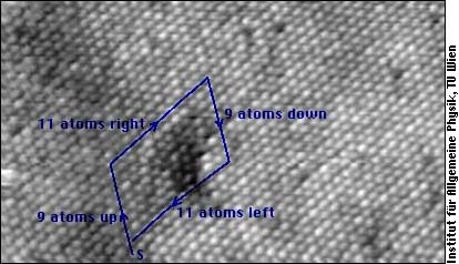
A dislocation is characterized by its Burgers vector: If you imagine going around the dislocation line, and exactly going back as many atoms in each direction as you have gone forward, you will not come back to the same atom where you have started. The Burgers vector points from start atom to the end atom of your journey (This "journey" is called Burgers circuit in dislocation theory).

In this electron microscope image of the surface of a crystal, you see point defects and a Burger journey around an edge dislocation. The dislocation line is in the crystal, and the image shows its ending at the surface. A Burger vector is approximately perpendicular to the dislocation line, and the missing line of atoms is somewhere within the block of the Buerger journey.
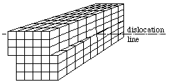
If the misalignment shifts a block of ions gradually downwards or upwards causing the formation of a screw like deformation, a screw dislocation is formed. The diagram here shows the idealized screw dislocation.

Line defects weakens the structure along a one-dimensional space, and the defects type and density affects the mechanical properties of the solids. Thus, formation and study of dislocations are particularly important for structural materials such as metals. This link gives some impressive images of dislocations. Chemical etching often reveal pits which are visible under small magnifications.
Example \(\PageIndex{1}\)
The Table of X-ray Crystallographic Data of Minerals (The CRC Handbook of Chemistry and Physics) list the following for bunsenite (NiO): Crystal system: cubic, structure type: rock salt, a = 4.177*10-8 cm. In the table of Physical Constant of Inorganic Compounds, the density of bunsenite (NiO) is 6.67g / cm3. From these values, evaluate the cell volume (volume of the unit cell), sum of Ni and O radii (rNi + rO), 2 Molar volumes, (X-ray) density, and the Schottky defect vacancy rate.
Solution
Actually, most of the required values have been listed in the table, but their evaluations illustrate the methods. These values are evaluated below:
Cell volume = a3
= (4.177*10-8)3
= 72.88*10-24 cm3
\[ r_{Ni}+r_O = \dfrac{a}{ 2} \nonumber \]
\[ = 2.088 \times 10^{-8} \nonumber \]
X-ray density = 4*(58.69+16.00) / (6.023*1023*72.88*10-24)
= 6.806 g / cm3,
Compared to the observed density = 6.67 g / cm3. The molar volumes (58.69+16.00) / density are thus
74.69 / 6.806 = 10.97 cm3; and 74.69 / 6.67 = 11.20 cm3
The vacancy rate = 6.806 - 6.67 / 6.806
= 0.02 (or 2%)
DISCUSSION
These methods are hints to assignments.
From the given conditions, we cannot calculate individual radii of Ni and O, but their sum is calculable.
Plane Defects
Plane defects occur along a 2-dimensional surface. The surface of a crystal is an obvious imperfection, because these surface atoms are different from those deep in the crystals. When a solid is used as a catalyst, the catalytic activity depends very much on the surface area per unit mass of the sample. For these powdery material, methods have been developed for the determination of unit areas per unit mass.
Another surface defects are along the grain boundaries. A grain is a single crystal. If many seeds are formed when a sample starts to crystallize, each seed grow until they meet at the boundaries. Properties along these boundaries are different from the grains. A third plane defects are the stacking faults. For example, in the close packing arrangement, the adjancent layers always have the AB relationship. In a ccp (fcc) close packing sequence, ...ABCABC..., one of the layer may suddenly be out of sequence, and become ..ABABCABC.... Similarly, in the hcp sequence, there is a possibility that one of the layer accidentally startes in the C location and resulting in the formation of a grain boundary.
How do impurities affect the structure and properties of a solid?
You already know that to obtain a perfectly pure substance is almost impossible. Purification is a costly process. In general, analytical reagent-grade chemicals are of high purity, and yet few of them are better than 99.9% pure. This means that a foreign atom or molecule is present for every 1000 host atoms or molecules in the crystal. Perhaps the most demanding of purity is in the electronic industry. Silicon crystals of 99.999 (called 5 nines) or better are required for IC chips productions. These crystal are doped with nitrogen group elements of P and As or boron group elements B, Al etc to form n- aand p-type semiconductors. In these crystals, the impurity atom substitute atoms of the host crystals.
Presence minute foreign atoms with one electron more or less than the valence four silicon and germanium host atoms is the key of making n- and p-type semiconductors. Having many semiconductors connected in a single chip makes the integrated circuit a very efficient information processor. The electronic properties change dramatically due to these impurities. This is further described in Inorganic Chemistry by Swaddle.
In other bulk materials, the presence of impurity usually leads to a lowering of melting point. For example, Hall and Heroult tried to electrolyze natural aluminum compounds. They discovered that using a 5% mixture of Al2O3 (melting point 273 K) in cryolite Na3AlF6 (melting point 1273 K) reduced the melting point to 1223 K, and that enabled the production of aluminum in bulk. Recent modifications lowered melting temperatures below 933 K. Some types of glass are made by mixing silica (SiO2), alumina (Al2O3), calcium oxide (CaO), and sodium oxide (Na2O). They are softer, but due to lower melting points, they are cheaper to produce.
Color centers and how do they affect electric conductivity of solids?
Color centers are imperfections in crystals that cause color (defects that cause color by absorption of light). Due to defects, metal oxides may also act as semiconductors, because there are many different types of electron traps. Electrons in defect region only absorb light at certain range of wavelength. The color seen are due to lights not absorbed. For example, a diamond with C vacancies (missing carbon atoms) absorbs light, and these centers give green color as shown here. Replacement of Al3+ for Si4+ in quartz give rise to the color of smoky quartz.
A high temperature phase of ZnOx, (x < 1), has electrons in place of the O2- vacancies. These electrons are color centers, often referred to as F-centers (from the German word farben meaning color). Similarly, heating of ZnS to 773 K causes a loss of sulfur, and these material fluoresces strongly in ultraviolet light. Some non-stoichiometric solids are engineered to be n-type or p-type semiconductors. Nickel oxide NiO gain oxygen on heating in air, resulting in having Ni3+ sites acting as electron trap, a p-type semiconductor. On the other hand, ZnO lose oxygen on heating, and the excess Zn metal atoms in the sample are ready to give electrons. The solid is an n-type semiconductor.
Questions
- Why does the density of water decreases when the temperature decreases from 277 to 273 K?
- What type of defects is due to misplaced atoms or ions and vacancies of the same in a crystalline material.
- What defects reduce the density of a solid?
- What type of material do the fuel cell and battery technologies need to separate the electrodes?
Solutions
- Hint: Due to the formation of flickering clusters.
Skill -
Correlate properties of a material to its structure. - Hint: Frenkel defects.
Skill -
Explain Frendel and Schottky defects. - Hint: Vacancies of Schottky defects reduce the density.
Skill -
Correlate properties of a material to its structure. - Hint: Ionic conductors.
Skill -
Specify the desirable properties of a material.
Contributors and Attributions
Chung (Peter) Chieh (Professor Emeritus, Chemistry @ University of Waterloo)

