11.2: Physics and Length Scales- Cavity Laser, Coulomb Blockade, Nanoscale Magnets
- Last updated
- Save as PDF
- Page ID
- 226765
The special properties of nanomaterials do not derive from different laws of physics, which are the same for objects large and small. For example, Newton's second law (\(F = ma\)), Coulomb's law (\(E= \frac{q_{1}q_{2}}{4 \pi \varepsilon_{0}r}\)), and the laws of energy and momentum conservation are the same for buckyballs (C60) and full-size soccer balls. Nevertheless, the physics of electrons, atoms, and photons naturally produce characteristic length scales, some of which we have already seen. For example, in Chapter 6 we discovered that the mean free path of an electron in a good metal is about 40 nm. In Chapter 10, we learned that the Bohr radius of an electron or hole in doped Si is about 4 nm, and that the coherence length of Cooper pairs in semiconductors is somewhere between a few nm and 1 µm. When objects become small relative to these characteristic lengths, their physical properties change in interesting ways. Materials that exist at the relevant length scale are called mesoscopic (meso = "between," scopic = "size") meaning that they cross over from one kind of behavior - the bulk behavior of large objects - to another. This length scale is different for different kinds of properties, but for many it happens between 1 and 100 nm. We illustrate this point with a few examples.
The cavity laser
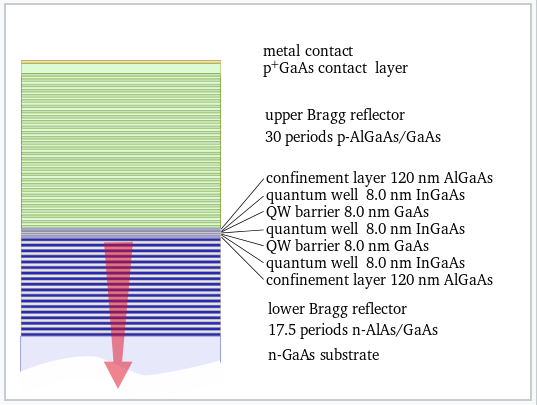
A vertical cavity surface-emitting laser (or VCSEL) is a semiconductor-based device that emits light in the vertical direction relative to the plane of the chip. These devices are being developed and used for high power applications such as laser surgery, infrared illumination for military surveillance, and laser cutting tools. The basic design of a VCSEL is shown at the right. The VCSEL is basically a light-emitting diode, incorporating p-type and n-type regions of the III-V semiconductor (Al,Ga)As. However, it has two special features. First, the refractive index of the semiconductor is modulated above and below the junction to make Bragg mirrors. These mirrors reflect light emitted in the junction, so that the photon density becomes very high there, a necessary condition for stimulated emission and lasing. The Bragg mirror stack is asymmetric (thinner on the bottom), so that light can escape from the junction in one direction only. Second, the junction itself consists of a thin "quantum well" layer of (In,Ga)As, a III-V semiconductor with a smaller band gap than the surrounding (Al,Ga)As layers.
|
A VCSEL device structure. This is a bottom-emitting multiple-quantum-well VCSEL. |
The quantum well structure, the band diagram of which is illustrated at the left, is the nanoscale part of the laser. The energies of the conduction and valence bands of (Al,Ga)As flank those of the thin (In,Ga)As layer. Therefore, electrons and holes injected into that layer cannot escape: electrons in (In,Ga)As do not have enough energy to climb "up" to the conduction band of (Al,Ga)As and holes cannot climb "down." Electrons confined to such a small well behave as a particle-in-a-box (as we learned in the context of electrides in Chapter 9).
The electron has a kinetic energy defined by the equation:
\[KE= \frac{h^{2}n^{2}}{8mL^{2}}\]
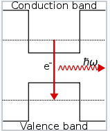 |
We can calculate the energy difference between the lowest (n=1) and next lowest (n=2) levels, which is inversely proportional to the square of the thickness (L) of the (In,Ga)As layer. In this calculation we need to use the effective mass of the electron in (In,Ga)As, which is about 7% of the electron rest mass[1]. With an 8 nm thick layer, this energy is:
\[E = \frac{(2^{2}-1^{2})(6.626 \cdot 10^{-34} Js)^{2}}{8 \cdot 0.07 \cdot (9.1 \cdot 10^{-31} kg)(8 \cdot 10^{-9} m)^{2}} = 4.0 \cdot 10^{-20} J = 0.25eV\]
The VCSEL cavity will thus have a resonant energy of 0.25 eV and emit photons at this energy in the infrared (λ ≈ 5000 nm). Note that because of the inverse square dependence of the cavity energy on layer thickness, lasers based on this design can only function at nanoscale dimensions. When the cavity is three times thicker, its resonant energy becomes comparable to the thermal energy at room temperature (kT = 0.026 eV), and the lasing effect is thermally "washed out."
Coulomb blockade
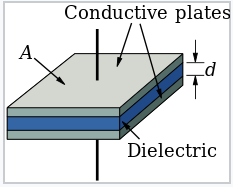
A capacitor is a (macroscopic) device that stores electrical charge. The basic structure of a capacitor is shown at the right. When a voltage is applied to such a device, it develops a charge (± Q) on the two plates that is proportional to the voltage:
\[C= \frac{Q}{V}\]
|
Basic design of a parallel plate capacitor of area A and with a dielectric thickness of d |
The magnitude of the capacitance C is determined by the permittivity ε and the dimensions of the dielectric layer, A and d.
\[C= \frac{\varepsilon A}{d}\]
We can also calculate the work done in charging the capacitor up (i.e., the energy stored by charging the capacitor) by integrating the voltage times the charge:
\[E = int^{Q}_{0} V(q)dq = \int^{Q}_{0} \frac{q}{C} dq = \frac{1}{2} \frac{Q^{2}}{C} = \frac{1}{2}CV^{2} = \frac{1}{2}VQ\]
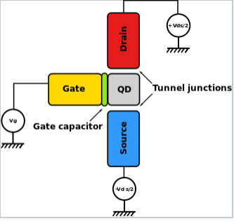
Now it is interesting to ask, what happens to a capacitor when we make it very small? This is of particular interest in a device called a single electron transistor, a schematic diagram of which is shown at the right. The metallic gate lead is separated from a "quantum dot," which can be a metal or semiconductor particle, by a thin dielectric layer. This metal-dielectric-metal sandwich acts as a capacitor, and from the equation above, the energy needed to charge it by a single electron (Q = e) is:
\[E= \frac{e^{2}}{2C}\]
where e is the charge of the electron, 1.602 x 10⁻¹⁹ Coulomb. If the gate width and lateral dimensions are very small - say 2 nm as is readily achievable in self-assembled Coulomb blockade devices[2][3] - then for a typical insulating dielectric, a voltage of about 200 mV is needed to charge the quantum dot by a single electron. Again, this effect is unique to the nanoscale, because a 10 times larger device area would make the single-electron charging voltage about 20 mV, which is smaller than the thermal energy kT (26 meV). Thus for devices larger than about 5-6 nm, individual electron charging events are washed out at room temperature by thermal fluctuations.
|
Schematic of a single-electron transistor. |
How can a nanoscale capacitor like this act as a transistor, which functions as a switch in an electrical circuit? The effect comes from the mutual repulsion of electrons. An electron on the quantum dot repels any other electron that would be forced onto it by applying a small voltage between the source and the drain. Hence the conductance of the quantum dot is very low at a gate bias of zero volts, or at any gate bias (200, 400, 600 mV...) that places an integer number (1, 2, 3,...) of electrons on the dot. But halfway in between these voltages (e.g., at 100, 300, 500 mV) the energy is the same whether there are n or n+1 electrons on the dot. This means that electrons can hop on and off without changing their energy, i.e., they can tunnel through the dot from source to drain. This effect gives peaks in the conductance of the dot at regular steps in the gate voltage. In effect, the gate can act as a switch, as in a conventional field-effect transistor. Single-electron transistors are being researched as ultra-sensitive electrometers and single-molecule chemical sensors, since a tiny change in the electrostatic environment of the dot can switch the device on or off.
Nanoscale magnets
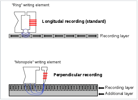
Ferro- and ferrimagnetic materials such as iron and chromium oxide are used for digitial storage of information in hard disks. The individual memory bits, which can be oriented perpendicular or parallel to the plane of the disk as shown at the right, store a logical "0" or "1" depending on the orientation of their magnetic dipole. To be useful, this information must be non-volatile, i.e., the magnetic bit must retain its polarization in the absence of an applied field from the read/write head.
|
Longitudinal and perpendicular recording, two types of writing heads on a hard disk. |
The storage density of such magnetic memories is impressive. A 2.5" hard drive can now store 1 TB of information, using rod-shaped magnetic grains that are approximately 0.5 µm long. We now have good synthetic methods for making these same materials as crystals with dimensions of only a few nanometers. Why aren't those nanocrystals used to make even more dense memory disks?
The reason is that the energy needed to flip the magnetization (i.e., to turn a "0" into a "1" and vice-versa) is strongly size-dependent. For a ferro- or ferrimagnet this energy is equal to Mr3, where M is the magnetic energy per unit volume and r is the characteristic dimension (e.g., the length of the edge of a cube, or the diameter of a sphere) of the magnetic grain. For typical materials such as iron, this energy becomes comparable to kT when r is about 3-5 nm. Such small particles are superparamagnetic, meaning that they still have a large magnetic moment because of the ordering of their spins, but they do not retain a permanent polarization in the absence of an applied magnetic field. Superparamagnetic particles are thus not useful for magnetic memories, but they are interesting and practical in other ways, for example in ferrofluids, magnetic resonance imaging (MRI), and some emerging medical diagnostic and therapeutic applications.
|
A ferrofluid containing superparamagnetic Fe3O4 nanoparticles, which are coated with oleic acid and suspended in oil, in the field of a strong permanent magnet. |
In these three illustrative examples (involving light emission, electronic conduction, and magnetic behavior), the transition to new properties involves a crossover in which the characteristic energy of the system is comparable to the thermal energy kT. It just so happens that for many physical phenomena, this crossover occurs on the length scale of nanometers.


