
6.2: Low Energy Electron Diffraction (LEED)
- Page ID
- 25388

\( \newcommand{\vecs}[1]{\overset { \scriptstyle \rightharpoonup} {\mathbf{#1}} } \)
\( \newcommand{\vecd}[1]{\overset{-\!-\!\rightharpoonup}{\vphantom{a}\smash {#1}}} \)
\( \newcommand{\id}{\mathrm{id}}\) \( \newcommand{\Span}{\mathrm{span}}\)
( \newcommand{\kernel}{\mathrm{null}\,}\) \( \newcommand{\range}{\mathrm{range}\,}\)
\( \newcommand{\RealPart}{\mathrm{Re}}\) \( \newcommand{\ImaginaryPart}{\mathrm{Im}}\)
\( \newcommand{\Argument}{\mathrm{Arg}}\) \( \newcommand{\norm}[1]{\| #1 \|}\)
\( \newcommand{\inner}[2]{\langle #1, #2 \rangle}\)
\( \newcommand{\Span}{\mathrm{span}}\)
\( \newcommand{\id}{\mathrm{id}}\)
\( \newcommand{\Span}{\mathrm{span}}\)
\( \newcommand{\kernel}{\mathrm{null}\,}\)
\( \newcommand{\range}{\mathrm{range}\,}\)
\( \newcommand{\RealPart}{\mathrm{Re}}\)
\( \newcommand{\ImaginaryPart}{\mathrm{Im}}\)
\( \newcommand{\Argument}{\mathrm{Arg}}\)
\( \newcommand{\norm}[1]{\| #1 \|}\)
\( \newcommand{\inner}[2]{\langle #1, #2 \rangle}\)
\( \newcommand{\Span}{\mathrm{span}}\) \( \newcommand{\AA}{\unicode[.8,0]{x212B}}\)
\( \newcommand{\vectorA}[1]{\vec{#1}} % arrow\)
\( \newcommand{\vectorAt}[1]{\vec{\text{#1}}} % arrow\)
\( \newcommand{\vectorB}[1]{\overset { \scriptstyle \rightharpoonup} {\mathbf{#1}} } \)
\( \newcommand{\vectorC}[1]{\textbf{#1}} \)
\( \newcommand{\vectorD}[1]{\overrightarrow{#1}} \)
\( \newcommand{\vectorDt}[1]{\overrightarrow{\text{#1}}} \)
\( \newcommand{\vectE}[1]{\overset{-\!-\!\rightharpoonup}{\vphantom{a}\smash{\mathbf {#1}}}} \)
\( \newcommand{\vecs}[1]{\overset { \scriptstyle \rightharpoonup} {\mathbf{#1}} } \)
\( \newcommand{\vecd}[1]{\overset{-\!-\!\rightharpoonup}{\vphantom{a}\smash {#1}}} \)
\(\newcommand{\avec}{\mathbf a}\) \(\newcommand{\bvec}{\mathbf b}\) \(\newcommand{\cvec}{\mathbf c}\) \(\newcommand{\dvec}{\mathbf d}\) \(\newcommand{\dtil}{\widetilde{\mathbf d}}\) \(\newcommand{\evec}{\mathbf e}\) \(\newcommand{\fvec}{\mathbf f}\) \(\newcommand{\nvec}{\mathbf n}\) \(\newcommand{\pvec}{\mathbf p}\) \(\newcommand{\qvec}{\mathbf q}\) \(\newcommand{\svec}{\mathbf s}\) \(\newcommand{\tvec}{\mathbf t}\) \(\newcommand{\uvec}{\mathbf u}\) \(\newcommand{\vvec}{\mathbf v}\) \(\newcommand{\wvec}{\mathbf w}\) \(\newcommand{\xvec}{\mathbf x}\) \(\newcommand{\yvec}{\mathbf y}\) \(\newcommand{\zvec}{\mathbf z}\) \(\newcommand{\rvec}{\mathbf r}\) \(\newcommand{\mvec}{\mathbf m}\) \(\newcommand{\zerovec}{\mathbf 0}\) \(\newcommand{\onevec}{\mathbf 1}\) \(\newcommand{\real}{\mathbb R}\) \(\newcommand{\twovec}[2]{\left[\begin{array}{r}#1 \\ #2 \end{array}\right]}\) \(\newcommand{\ctwovec}[2]{\left[\begin{array}{c}#1 \\ #2 \end{array}\right]}\) \(\newcommand{\threevec}[3]{\left[\begin{array}{r}#1 \\ #2 \\ #3 \end{array}\right]}\) \(\newcommand{\cthreevec}[3]{\left[\begin{array}{c}#1 \\ #2 \\ #3 \end{array}\right]}\) \(\newcommand{\fourvec}[4]{\left[\begin{array}{r}#1 \\ #2 \\ #3 \\ #4 \end{array}\right]}\) \(\newcommand{\cfourvec}[4]{\left[\begin{array}{c}#1 \\ #2 \\ #3 \\ #4 \end{array}\right]}\) \(\newcommand{\fivevec}[5]{\left[\begin{array}{r}#1 \\ #2 \\ #3 \\ #4 \\ #5 \\ \end{array}\right]}\) \(\newcommand{\cfivevec}[5]{\left[\begin{array}{c}#1 \\ #2 \\ #3 \\ #4 \\ #5 \\ \end{array}\right]}\) \(\newcommand{\mattwo}[4]{\left[\begin{array}{rr}#1 \amp #2 \\ #3 \amp #4 \\ \end{array}\right]}\) \(\newcommand{\laspan}[1]{\text{Span}\{#1\}}\) \(\newcommand{\bcal}{\cal B}\) \(\newcommand{\ccal}{\cal C}\) \(\newcommand{\scal}{\cal S}\) \(\newcommand{\wcal}{\cal W}\) \(\newcommand{\ecal}{\cal E}\) \(\newcommand{\coords}[2]{\left\{#1\right\}_{#2}}\) \(\newcommand{\gray}[1]{\color{gray}{#1}}\) \(\newcommand{\lgray}[1]{\color{lightgray}{#1}}\) \(\newcommand{\rank}{\operatorname{rank}}\) \(\newcommand{\row}{\text{Row}}\) \(\newcommand{\col}{\text{Col}}\) \(\renewcommand{\row}{\text{Row}}\) \(\newcommand{\nul}{\text{Nul}}\) \(\newcommand{\var}{\text{Var}}\) \(\newcommand{\corr}{\text{corr}}\) \(\newcommand{\len}[1]{\left|#1\right|}\) \(\newcommand{\bbar}{\overline{\bvec}}\) \(\newcommand{\bhat}{\widehat{\bvec}}\) \(\newcommand{\bperp}{\bvec^\perp}\) \(\newcommand{\xhat}{\widehat{\xvec}}\) \(\newcommand{\vhat}{\widehat{\vvec}}\) \(\newcommand{\uhat}{\widehat{\uvec}}\) \(\newcommand{\what}{\widehat{\wvec}}\) \(\newcommand{\Sighat}{\widehat{\Sigma}}\) \(\newcommand{\lt}{<}\) \(\newcommand{\gt}{>}\) \(\newcommand{\amp}{&}\) \(\definecolor{fillinmathshade}{gray}{0.9}\)LEED is the principal technique for the determination of surface structures. It may be used in one of two ways:
- Qualitatively: where the diffraction pattern is recorded and analysis of the spot positions yields information on the size, symmetry and rotational alignment of the adsorbate unit cell with respect to the substrate unit cell.
- Quantitatively: where the intensities of the various diffracted beams are recorded as a function of the incident electron beam energy to generate so-called I-V curves which, by comparison with theoretical curves, may provide accurate information on atomic positions.
In this section, we will only consider the qualitative application of this experimental technique.
Experimental Details
The LEED experiment uses a beam of electrons of a well-defined low energy (typically in the range 20 - 200 eV) incident normally on the sample. The sample itself must be a single crystal with a well-ordered surface structure in order to generate a back-scattered electron diffraction pattern. A typical experimental set-up is shown below.
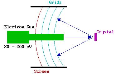
Only the elastically-scattered electrons contribute to the diffraction pattern ; the lower energy (secondary) electrons are removed by energy-filtering grids placed in front of the fluorescent screen that is employed to display the pattern.
Basic Theory of LEED
By the principles of wave-particle duality, the beam of electrons may be equally regarded as a succession of electron waves incident normally on the sample. These waves will be scattered by regions of high localised electron density, i.e. the surface atoms, which can therefore be considered to act as point scatterers.
The wavelength of the electrons is given be the de Broglie relation:
\[ \lambda = \dfrac{h}{p}\]
where \(\lambda\) is the electron wavelength and \(p\) is its momentum.
Now,
\[p = mv = \sqrt{2mE_k} = \sqrt{2m e V} \]
where
- m - mass of electron [ kg ]
- v - velocity [ m s-1 ]
- Ek - kinetic energy
- e - electronic charge
- V - acceleration voltage ( = energy in eV )
⇒ Wavelength,
\[\lambda = \dfrac{h}{\sqrt{2meV}}\]
![]() What is the wavelength of electrons of energy 20 eV ?
What is the wavelength of electrons of energy 20 eV ?
![]() What is the wavelength of electrons of energy 200 eV ?
What is the wavelength of electrons of energy 200 eV ?
(Useful information: h = 6.62 x 10⁻³⁴ J s, e = 1.60 x 10⁻¹⁹ C, me = 9.11 x 10⁻³¹ kg ).
From the above examples the range of wavelengths of electrons employed in LEED experiments is seen to be comparable with atomic spacings, which is the necessary condition for diffraction effects associated with atomic structure to be observed.
Consider, first, a one dimensional (1-D) chain of atoms (with atomic separation a ) with the electron beam incident at right angles to the chain. This is the simplest possible model for the scattering of electrons by the atoms in the topmost layer of a solid; in which case the diagram below would be representing the solid in cross-section with the electron beam incident normal to the surface from the vacuum above.
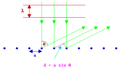
If you consider the backscattering of a wavefront from two adjacent atoms at a well-defined angle, \(θ\), to the surface normal then it is clear that there is a "path difference" (d) in the distance the radiation has to travel from the scattering centres to a distant detector (which is effectively at infinity) - this path difference is best illustrated by considering two "ray paths" such as the right-hand pair of green traces in the above diagram.
The size of this path difference is a sin θ and this must be equal to an integral number of wavelengths for constructive interference to occur when the scattered beams eventually meet and interfere at the detector i.e.
\[d = a sin θ = n λ\]
|
where: |
λ - wavelength n - integer (..-1, 0, 1, 2,.. ) |
For two isolated scattering centres the diffracted intensity varies slowly between zero (complete destructive interference ; d = (n + ½) λ ) and its maximum value (complete constructive interference ; d = n λ ) - with a large periodic array of scatterers, however, the diffracted intensity is only significant when the "Bragg condition"
\[a sin θ = n λ\]
is satisfied exactly. The diagram below shows a typical intensity profile for this case.
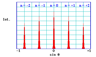
There are a number of points worth noting from this simple 1-D model
- the pattern is symmetric about θ = 0 (or sin θ = 0)
- sin θ is proportional to 1 / V 1/2 (since λ is proportional to 1 / V 1/2 )
- sin θ is inversely proportional to the lattice parameter, a
The aforementioned points are in fact much more general - all surface diffraction patterns show a symmetry reflecting that of the surface structure, are centrally symmetric, and of a scale showing an inverse relationship to both the square root of the electron energy and the size of the surface unit cell.
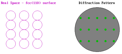
As an example we can look at the LEED pattern from an fcc(110) surface. In the diagram below the surface atomic structure is shown on the left in plan view, as if you are viewing it from the position of the electron gun in the LEED experiment (albeit greatly magnified). The primary electron beam would then be incident normally on this surface as if fired from your current viewpoint and the diffracted beams would be scattered from the surface back towards yourself. The diffraction pattern on the right illustrates how these diffracted beams would impact upon the fluorescent screen.
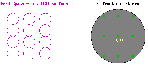
The pattern shows the same rectangular symmetry as the substrate surface but is "stretched" in the opposite sense to the real space structure due to the reciprocal dependence upon the lattice parameter. The pattern is also centrosymmetric about the (00) beam - this is the central spot in the diffraction pattern corresponding to the beam that is diffracted back exactly normal to the surface (i.e. the n = 0 case in our 1-D model).
The above illustration of the diffraction pattern shows only the "first-order" beams i.e. it is representative of the diffraction pattern visible at low energies when only for n = 1 is the angle of diffraction, θ, sufficiently small for the diffracted beam to be incident on the display screen.
By contrast, the diagram below shows the diffraction pattern that might be expected if the energy of the incident electrons is doubled - some of the second order spots are now visible and the pattern as a whole has apparently contracted in towards the central (00) spot.
This is what the real diffraction patterns might look like … ![]()
In the case of such simple LEED patterns, it is possible to explain the diffraction pattern in terms of scattering from rows of atoms on the surface. For example, the rows of atoms running vertically on the screen would give rise to a set of diffracted beams in the horizontal plane, perpendicular to the rows, thus leading to the row of spots running in a line horizontally across the diffraction pattern through the (00) spot. The further the rows are apart, then the closer in are the diffracted beams to the central (00) beam. This is, however, a far from satisfactory method of explaining LEED patterns from surfaces.
A much better method of looking at LEED diffraction patterns involves using the concept of reciprocal space: more specifically, it can be readily shown that -
" The observed LEED pattern is a (scaled) representation of the reciprocal net of the pseudo-2D surface structure "
(No proof given !)
The reciprocal net is determined by (defined by) the reciprocal vectors:
a1* & a2* (for the substrate) and b1* & b2* (for the adsorbate)
Initially we will consider just the substrate. The reciprocal vectors are related to the real space unit cell vectors by the scalar product relations:
a1 . a2* = a1* . a2 = 0
and
a1 . a1* = a2 . a2* = 1
For those not too keen on vector algebra these mean that:
- a1 is perpendicular to a2*, and a2 is perpendicular to a1*
- there is an inverse relationship between the lengths of a1 and a1* (and a2 and a2* ) of the form:
|a1| = 1 / ( |a1*| cos A ) , where A is the angle between the vectors a1 and a1*.
Note: when A = 0 degrees (cos A = 1) this simplifies to a simple reciprocal relationship between the lengths a1 and a1*.
Exactly analogous relations hold for the real space and reciprocal vectors of the adsorbate overlayer structure: b1, b1*, b2 and b2* .
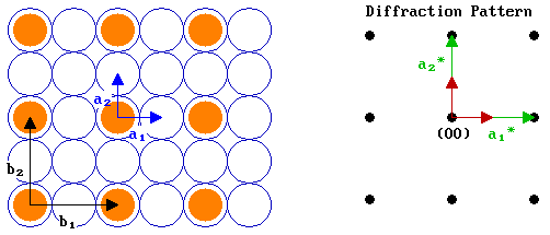
To a first approximation, the LEED pattern for a given surface structure may be obtained by superimposing the reciprocal net of the adsorbate overlayer (generated from b1* and b2* ) on the reciprocal net of the substrate (generated from a1* and a2* )
Let us now look at an example - the diagram below shows an fcc(100) surface (again in plan view) and its corresponding diffraction pattern (i.e. the reciprocal net) .

We can demonstrate how these reciprocal vectors can be determined by working through the problem in a parallel fashion for the two vectors:
|
a1* must be perpendicular to a2 |
a2* must be perpendicular to a1 |
|
|
⇒ |
a1* is parallel to a1 |
a2* is parallel to a2 |
|
⇒ |
The angle, A, between a1 & a1* is zero |
The angle, A, between a2 & a2* is zero |
|
⇒ |
Hence, | a1*| = 1 / | a1 | |
Hence, | a2*| = 1 / | a2 | |
|
⇒ |
If we let | a1 | = 1 unit, then | a1*| = 1 unit. |
| a2 | = | a1 | = 1 unit, therefore | a2*| = 1 unit. |
Let us now add in an adsorbate overlayer - a primitive ( 2 x 2 ) structure with the adsorbed species shown bonded in on-top sites - and apply the same logic as just used above to determine the reciprocal vectors, b1* and b2*, for this overlayer.
|
b1* must be perpendicular to b2 |
b2* must be perpendicular to b1 |
|
|
⇒ |
b1* is parallel to b1 |
b2* is parallel to b2 |
|
⇒ |
The angle, B, between b1 & b1* is zero |
The angle, B, between b2 & b2* is zero |
|
⇒ |
Hence, | b1*| = 1 / | b1 | |
Hence, | b2*| = 1 / | b2 | |
|
⇒ |
| b1 | = 2| a1 | = 2 units; ∴ | b1*| = ½ unit. |
| b2 | = 2| a2 | = 2 units; ∴ | b2*| = ½ unit. |
All we have to do now is to generate the reciprocal net for the adsorbate using b1* and b2* (shown in red).

That's all there is to it !
For the second example, we will look at the c( 2 x 2 ) structure on the same fcc(100) surface. The diagram below shows both a real space c( 2 x 2 ) structure and the corresponding diffraction pattern:
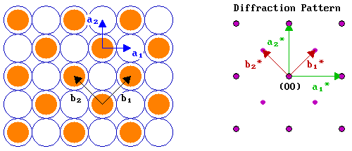
In many respects the analysis is very similar to that for the p( 2 x 2 ) structure, except that:
- | b1 | = | b2 | = √2 units ; consequently | b1*| = | b2*| = 1/√2 units.
- the vectors for the adsorbate overlayer are rotated with respect to those of the substrate by 45°.
Note that the c( 2 x 2 ) diffraction pattern can also be obtained from the pattern for the primitive structure by "missing out every alternate adsorbate-derived diffraction spot". This is a common feature of diffraction patterns arising from centered structures.