
31.9: The Structure of a Surface is Different from that of a Bulk Solid
- Page ID
- 14581
The kinetics and thermodynamics of the chemical and physical processes that occur on the surface of a solid are greatly dependent on the structure of the surface. Few, if any surfaces are perfectly flat, and thus the cavities, protrusions, ridges, and edges of the surface must be treated differently when studying chemisorption and physisorption. Several types of spectroscopies and microscopies are available to study the atomic-scale structure of surfaces.

Electron Microscopy
The two forms of electron microscopy which are commonly used to provide surface information are
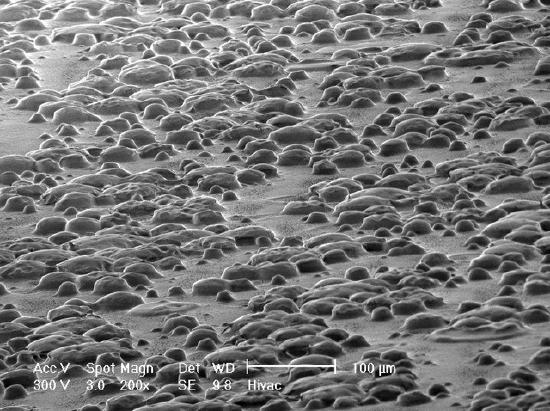
- Secondary Electron Microscopy ( SEM ): which provides a direct image of the topographical nature of the surface from all the emitted secondary electrons
- Scanning Auger Microscopy ( SAM ): which provides compositional maps of a surface by forming an image from the Auger electrons emitted by a particular element.
Both techniques employ the focusing of the probe beam (a beam of high-energy electrons, typically 10 - 50 keV in energy) to obtain spatial localization.
Secondary Electron Microscopy (SEM)
As the primary electron beam is scanned across the surface, electrons of a wide range of energies will be emitted from the surface in the region where the beam is incident. These electrons will include backscattered primary electrons and Auger electrons, but the vast majority will be secondary electrons formed in multiple inelastic scattering processes (these are the electrons that contribute to the background and are completely ignored in Auger spectroscopy). The secondary electron current reaching the detector is recorded and the microscope image consists of a "plot" of this current, I, against probe position on the surface. The contrast in the micrograph arises from several mechanisms, but first and foremost from variations in the surface topography. Consequently, the secondary electron micrograph is virtually a direct image of the real surface structure (Figure \(\PageIndex{1}\)).
The attainable resolution of the technique is limited by the minimum spot size that can be obtained with the incident electron beam, and ultimately by the scattering of this beam as it interacts with the substrate. With modern instruments, a resolution of better than 5 nm is achievable. This is more than adequate for imaging semiconductor device structures, for example, but insufficient to enable many supported metal catalysts to be studied in any detail.
Scanning Auger Microscopy ( SAM )
The incident primary electrons cause the ionization of atoms within the region illuminated by the focused beam. Subsequent relaxation of the ionized atoms leads to the emission of Auger electrons characteristic of the elements present in this part of the sample surface. As with SEM , the attainable resolution is again ultimately limited by the incident beam characteristics. More significantly, however, the resolution is also limited by the need to acquire sufficient Auger signal to form a respectable image within a reasonable time period, and for this reason, the instrumental resolution achievable is rarely better than about 15-20 nm.
Low-Energy Electron Diffraction (LEED) Spectroscopy
LEED is the principal technique for the determination of surface structures. It may be used in one of two ways:
- Qualitatively: where the diffraction pattern is recorded and analysis of the spot positions yields information on the size, symmetry, and rotational alignment of the adsorbate unit cell with respect to the substrate unit cell.
- Quantitatively: where the intensities of the various diffracted beams are recorded as a function of the incident electron beam energy to generate so-called I-V curves which, by comparison with theoretical curves, may provide accurate information on atomic positions.
The LEED experiment uses a beam of electrons of a well-defined low energy (typically in the range 20 - 200 eV) incident normally on the sample. The sample itself must be a single crystal with a well-ordered surface structure in order to generate a back-scattered electron diffraction pattern. A typical experimental setup is shown in figure \(\PageIndex{3}\) below.

Only the elastically-scattered electrons contribute to the diffraction pattern; the lower energy (secondary) electrons are removed by energy-filtering grids placed in front of the fluorescent screen that is employed to display the pattern.
As shown by the Bragg equation, for the electrons to be diffracted, the de Broglie wavelength of the electrons has to be less than 2\(d\), which is twice the distance between the atomic planes. The equation used to calculate the wavelength (in nm) of backscattered electrons that are accelarated by a potential, \(\phi\) is
\[\lambda = \left( \dfrac{1.504 \, V nm^2}{\phi} \right)^{1/2} \nonumber \]
Calculate the minimum acceleration voltage needed to observe electron diffraction from the surface of a crystal with an interplanar spacing of 0.1250 nm.
Solution
To observe diffraction, the wavelength must be less than 2\(d\), so \(\lambda\) must be less than 0.2500 nm. Therefore,
\[0.2500 \, nm = \left( \dfrac{1.504 \, V nm^2}{\phi} \right)^{1/2} \nonumber \]
\[\phi = \dfrac{1.504 \, V nm^2}{(0.2500 \, nm)^2} \nonumber \]
\[\phi = 24.06 V \nonumber \]
Contributors and Attributions
Roger Nix (Queen Mary, University of London)