
2.2: Bands of Orbitals in Solids
- Page ID
- 11573

Not only does the particle-in-a-box model offer a useful conceptual representation of electrons moving in polyenes, but it also is the zeroth-order model of band structures in solids. Let us consider a simple one-dimensional crystal consisting of a large number of atoms or molecules, each with a single orbital (the blue spheres shown below) that it contributes to the bonding. Let us arrange these building blocks in a regular lattice as shown in the Figure 2.5.
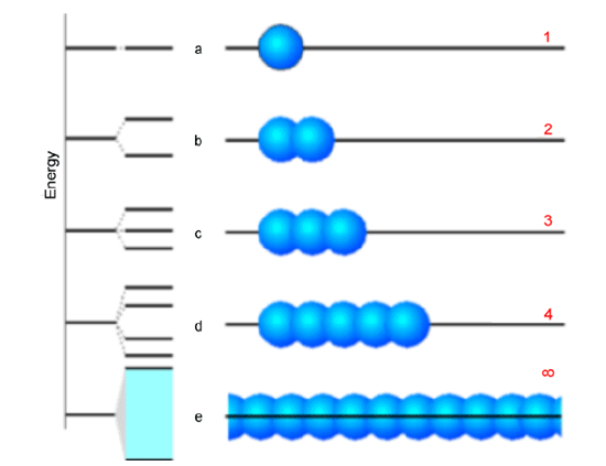
In the top four rows of this figure we show the case with 1, 2, 3, and 5 building blocks. To the left of each row, we display the energy splitting pattern into which the building blocks’ orbitals evolve as they overlap and form delocalized molecular orbitals. Not surprisingly, for \(n = 2\), one finds a bonding and an antibonding orbital. For \(n = 3\), one has a bonding, one non-bonding, and one antibonding orbital. Finally, in the bottom row, we attempt to show what happens for an infinitely long chain. The key point is that the discrete number of molecular orbitals appearing in the 1-5 orbital cases evolves into a continuum of orbitals called a band as the number of building blocks becomes large. This band of orbital energies ranges from its bottom (whose orbital consists of a fully in-phase bonding combination of the building block orbitals) to its top (whose orbital is a fully out-of-phase antibonding combination).
In Figure 2.6 we illustrate these fully bonding and fully antibonding band orbitals for two cases- the bottom involving s-type building block orbitals, and the top involving \(p_\sigma\)-type orbitals. Notice that when the energy gap between the building block \(s\) and \(p_\sigma\) orbitals is larger than is the dispersion (spread) in energy within the band of \(s\) or band of \(p_\sigma\) orbitals, a band gap occurs between the highest member of the \(s\) band and the lowest member of the \(p_\sigma\) band. The splitting between the \(s\) and \(p_\sigma\) orbitals is a property of the individual atoms comprising the solid and varies among the elements of the periodic table. For example, we teach students that the \(2s\)-\(2p\) energy gap in C is smaller than the \(3s\)-\(3p\) gap in Si, which is smaller than the \(4s\)-\(4p\) gap in Ge. The dispersion in energies that a given band of orbitals is split into as these atomic orbitals combine to form a band is determined by how strongly the orbitals on neighboring atoms overlap. Small overlap produces small dispersion, and large overlap yields a broad band. So, the band structure of any particular system can vary from one in which narrow bands (weak overlap) do not span the energy gap between the energies of their constituent atomic orbitals to bands that overlap strongly (large overlap).
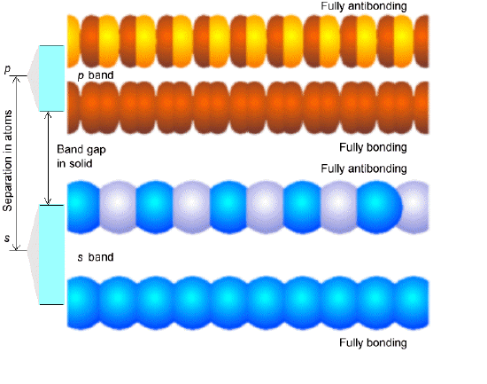
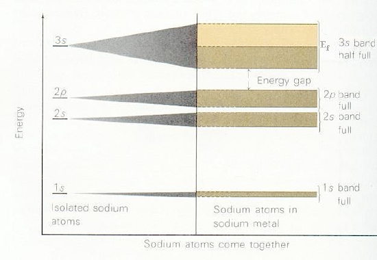
Depending on how many valence electrons each building block contributes, the various bands formed by overlapping the building-block orbitals of the constituent atoms will be filled to various levels. For example, if each building block orbital shown above has a single valence electron in an s-orbital (e.g., as in the case of the alkali metals), the s-band will be half filled in the ground state with a and b -paired electrons. Such systems produce very good conductors because their partially filled \(s\) bands allow electrons to move with very little (e.g., only thermal) excitation among other orbitals in this same band. On the other hand, for alkaline earth systems with two \(s\) electrons per atom, the s-band will be completely filled. In such cases, conduction requires excitation to the lowest members of the nearby p-orbital band. Finally, if each building block were an Al (3s2 3p1) atom, the s-band would be full and the p-band would be half filled. In Figure 2.6 a, we show a qualitative depiction of the bands arising from sodium atoms’ \(1s\), \(2s\), \(2p\), and \(3s\) orbitals. Notice that the \(1s\) band is very narrow because there is little coupling between neighboring \(1s\) orbitals, so they are only slightly stabilized or destabilized relative to their energies in the isolated Na atoms. In contrast, the \(2s\) and \(2p\) bands show greater dispersion (i.e., are wider), and the \(3s\) band is even wider. The \(1s\), \(2s\), and \(2p\) bands are full, but the \(3s\) band is half filled, as a result of which solid Na is a good electrical conductor.
In describing the band of states that arise from a given atomic orbital within a solid, it is common to display the variation in energies of these states as functions of the number of sign changes in the coefficients that describe each orbital as a linear combination of the constituent atomic orbitals. Using the one-dimensional array of \(s\) and \(p_{\sigma}\) orbitals shown in Figure 2.6 as an example,
- The lowest member of the band deriving from the \(s\) orbitals \[ \phi_o = s(1) + s(2) +s(3) + s(4) ... + s(N) \tag{2.1}\] is a totally bonding combination of all of the constituent \(s\) orbitals on the \(N\) sites of the lattice.
- The highest-energy orbital in this band \[\phi_N=s(1)- s(2) +s(3) - s(4) ... + s(N-1) + s(N) \tag{2.2}\] is a totally anti-bonding combination of the constituent \(s\) orbitals.
- Each of the intervening orbitals in this band has expansion coefficients that allow the orbital to be written as \[\phi_n = \sum_{j=1}^N \cos \left( \dfrac{n(j-1)\pi}{N}\right)s(j)\tag{2.3}.\] Clearly, for small values of \(n\), the series of expansion coefficients \(\cos \left( \dfrac{n(j-1)\pi}{N}\right) \tag{2.4}\) has few sign changes as the index \(j\) runs over the sites of the one-dimensional lattice. For larger n, there are more sign changes. Thus, thinking of the quantum number \(n\) as labeling the number of sign changes and plotting the energies of the orbitals (on the vertical axis) versus \(n\) (on the horizontal axis), we would obtain a plot that increases from \(n = 0\) to \(n =N\). In fact, such plots tend to display quadratic variation of the energy with \(n\). This observation can be understood by drawing an analogy between the pattern of sign changes belonging to a particular value of \(n\) and the number of nodes in the one-dimensional particle-in-a-box wave function, which also is used to model electronic states delocalized along a linear chain. As we saw in Chapter 1, the energies for this model system varied as \[ E= \dfrac{j^2\pi^2\hbar^2}{2mL^2} \tag{2.5}\] with \(j\) being the quantum number ranging from \(1\) to \(\infty\). The lowest-energy state, with \(j = 1\), has no nodes; the state with \(j = 2\) has one node, and that with \(j = n\) has \((n-1)\) nodes. So, if we replace \(j\) by \((n-1)\) and replace the box length \(L\) by \((NR)\), where \(R\) is the inter-atom spacing and \(N\) is the number of atoms in the chain, we obtain \[ E= \dfrac{(n-1)^2\pi^2\hbar^2}{2mN^2R^2}\] from which on can see why the energy can be expected to vary as \((n/N)^2\).
- In contrast for the \(p_{\sigma}\) orbitals, the lowest-energy orbital is \[\phi_o=p_{\sigma}(1)- p_{\sigma}(2) +p_{\sigma}(3) - p_{\sigma}(4) ... - p_{\sigma}(N-1) + p_{\sigma}(N) \tag{2.6}\] because this alternation in signs allows each orbital on one site to overlap in a bonding fashion with the orbitals on neighboring sites.
- Therefore, the highest-energy orbital in the band is \[\phi_o=p_{\sigma}(1) + p_{\sigma}(2) +p_{\sigma}(3) + p_{\sigma}(4) ... + p_{\sigma}(N-1) + p_{\sigma}(N) \tag{2.7}\] and is totally anti-bonding.
- The intervening members of this band have orbitals given by \[\phi_{N-n} = \sum_{j=1}^N \cos \left( \dfrac{n(j-1)\pi}{N}\right)s(j) \tag{2.3}\] with low \(n\) corresponding to high-energy orbitals (having few inter-atom sign changes but anti-bonding character) and high \(n\) to low-energy orbitals (having many inter-atom sign changes). So, in contrast to the case for the s-band orbitals, plotting the energies of the orbitals (on the vertical axis) versus \(n\) (on the horizontal axis), we would obtain a plot that decreases from \(n = 0\) to \(n =N\).
For bands comprised of \(p_{\pi}\) orbitals, the energies vary with the \(n\) quantum number in a manner analogous to how the \(s\) band varies because the orbital with no inter-atom sign changes is fully bonding. For two- and three-dimensional lattices comprised of s, p, and d orbitals on the constituent atoms, the behavior of the bands derived from these orbitals follows analogous trends. It is common to describe the sign alternations arising from site to site in terms of a so-called \(\textbf{k}\) vector. In the one-dimensional case discussed above, this vector has only one component with elements labeled by the ratio (\(n/N\)) whose value characterizes the number of inter-atom sign changes. For lattices containing many atoms, \(N\) is very large, so \(n\) ranges from zero to a very large number. Thus, the ratio (\(n/N\)) ranges from zero to unity in small fractional steps, so it is common to think of these ratios as describing a continuous parameter varying from zero to one. Moreover, it is convention to allow the \(n\) index to range from \(–N\) to \(+N\), so the argument \(n \pi /N\) in the cosine function introduced above varies from \(-\pi\) to \(+\pi\).
In two- or three-dimensions the \(\textbf{k}\) vector has two or three elements and can be written in terms of its two or three index ratios, respectively, as
\[\textbf{k}_2=\Big(\dfrac{n}{N},\dfrac{m}{M}\Big)\]
\[\textbf{k}_3=\Big(\dfrac{n}{N},\dfrac{m}{M},\dfrac{l}{L}\Big).\]
Here, \(N\), \(M\), and \(L\) would describe the number of unit cells along the three principal axes of the three-dimensional crystal; \(N\) and \(M\) do likewise in the two-dimensional lattice case.
In such two- and three- dimensional crystal cases, the energies of orbitals within bands derived from s, p, d, etc. atomic orbitals display variations that also reflect the number of inter-atom sign changes. However, now there are variations as functions of the (\(n/N\)), (\(m/M\)) and (\(l/L\)) indices, and these variations can display rather complicated shapes depending on the symmetry of the atoms within the underlying crystal lattice. That is, as one moves within the three-dimensional space by specifying values of the indices (\(n/N\)), (\(m/M\)) and (\(l/L\)), one can move throughout the lattice in different symmetry directions. It is convention in the solid-state literature to plot the energies of these bands as these three indices vary from site to site along various symmetry elements of the crystal and to assign a letter to label this symmetry element. The band that has no inter-atom sign changes is labeled as \(\Gamma\) (sometimes G) in such plots of band structures. In much of our discussion below, we will analyze the behavior of various bands in the neighborhood of the \(\Gamma\) point because this is where there are the fewest inter-atom nodes and thus the wave function is easiest to visualize.
Let’s consider a few examples to help clarify these issues. In Figure 2.6 b, where we see the band structure of graphene, you can see the quadratic variations of the energies with \(\textbf{k}\) as one moves away from the \(\textbf{k} = 0\) point labeled \(\Gamma\), with some bands increasing with \(\textbf{k}\) and others decreasing with \(\textbf{k}\).
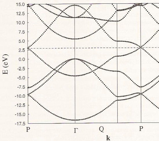
The band having an energy of ca. -17 eV at the \(\Gamma\) point originates from bonding interactions involving \(2s\) orbitals on the carbon atoms, while those having energies near 0 eV at the \(\Gamma\) point derive from carbon \(2p_\sigma\) bonding interactions. The parabolic increase with \(\textbf{k}\) for the \(2s\)-based and decrease with \(\textbf{k}\) for the \(2p_\sigma\)-based orbitals is clear and is expected based on our earlier discussion of how \(\sigma\) and \(p_{\sigma}\) bands vary with \(\textbf{k}\). The band having energy near -4 eV at the \(\Gamma\) point involves \(2p_\pi\) orbitals involved in bonding interactions, and this band shows a parabolic increase with \(\textbf{k}\) as expected as we move away from the \(\Gamma\) point. These are the delocalized \(\pi\) orbitals of the graphene sheet. The anti-bonding \(2p_\pi\) band decreases quadratically with \(\textbf{k}\) and has an energy of ca. 15 eV at the \(\Gamma\) point. Because there are two atoms per unit cell in this case, there are a total of eight valence electrons (four from each carbon atom) to be accommodated in these bands. The eight carbon valence electrons fill the bonding \(2s\) and two \(2p_\sigma\) bands fully as well as the bonding \(2p_\pi\) band. Only along the direction labeled P in Figure 2.6b do the bonding and anti-bonding \(2p_\pi\) bands become degenerate (near 2.5 eV); the approach of these two bands is what allows graphene to be semi-metallic (i.e., to conduct at modest temperatures- high enough to promote excitations from the bonding \(2p_\pi\) to the anti-bonding \(2p_\pi\) band).
It is interesting to contrast the band structure of graphene with that of diamond, which is shown in Figure 2. 6 c.
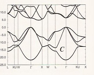
The band having an energy of ca. – 22 eV at the \(\Gamma\) point derives from \(2s\) bonding interactions, and the three bands near 0 eV at the \(\Gamma\) point come from \(2p_\sigma\) bonding interactions. Again, each of these bands displays the expected parabolic behavior as functions of \(\textbf{k}\). In diamond’s two interpenetrating face centered cubic structure, there are two carbon atoms per unit cell, so we have a total of eight valence electrons to fill the four bonding bands. Notice that along no direction in \(\textbf{k}\)-space do these filled bonding bands become degenerate with or are crossed by any of the other bands. The other bands remain at higher energy along all \(\textbf{k}\)-directions, and thus there is a gap between the bonding bands and the others is large (ca. 5 eV or more along any direction in \(\textbf{k}\)-space). This is why diamond is an insulator; the band gap is very large.
Finally, let’s compare the graphene and diamond cases with a metallic case such as shown in Figure 2. 6 d for Al and for Ag.
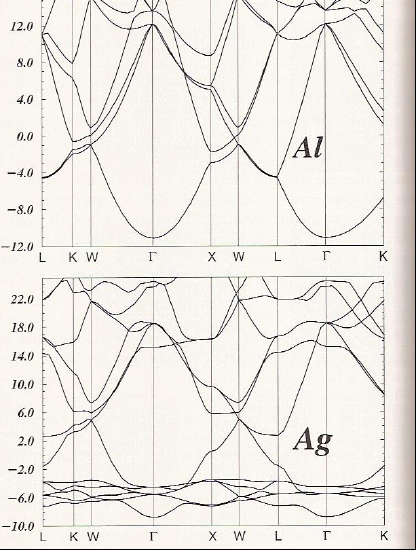
For Al and Ag, there is one atom per unit cell, so we have three valence electrons (3s23p1) and eleven valence electrons (3d104s1), respectively, to fill the bands shown in Figure 2.6d. Focusing on the \(\Gamma\) points in the Al and Ag band structure plots, we can say the following:
- For Al, the \(3s\)-based band near -11 eV is filled and the three \(3p\)-based bands near 11 eV have an occupancy of 1/6 (i.e., on average there is one electron in one of these three bands each of which can hold two electrons).
- The \(3s\) and \(3p\) bands are parabolic with positive and negative curvature, respectively.
- Along several directions (e.g. \(K\), \(W\), \(X\), \(W\), \(L\)) there are crossings among the bands; these crossings allow electrons to be promoted from occupied to previously unoccupied bands. The partial occupancy of the \(3p\) bands and the multiple crossings of bands are what allow Al to show metallic behavior.
- For Ag, there are six bands between -4 eV and -8 eV. Five of these bands change little with \(\textbf{k}\), and one shows somewhat parabolic dependence on \(\textbf{k}\). The former five derive from \(4d\) atomic orbitals that are contracted enough to not allow them to overlap much, and the latter is based on \(5s\) bonding orbital interaction.
- Ten of the valence electrons fill the five \(4d\) bands, and the eleventh resides in the 5s-based bonding band.
- If the five \(4d\)-based bands are ignored, the remainder of the Ag band structure looks a lot like that for Al. There are numerous band crossings that include, in particular, the half-filled \(5s\) band. These crossings and the partial occupancy of the \(5s\) band cause Ag to have metallic character.
One more feature of band structures that is often displayed is called the band density of states. An example of such a plot is shown in Figure 2.6 e for the TiN crystal.
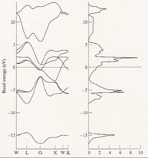
The density of states at energy \(E\) is computed by summing all those orbitals having an energy between \(E\) and \(E + dE\). Clearly, as seen in Figure 2.6e, for bands in which the orbital energies vary strongly with \(\textbf{k}\) (i.e., so-called broad bands), the density of states is low; in contrast, for narrow bands, the density of states is high. The densities of states are important because their energies and energy spreads relate to electronic spectral features. Moreover, just as gaps between the highest occupied bands and the lowest unoccupied bands play central roles in determining whether the sample is an insulator, a conductor, or a semiconductor, gaps in the density of states suggest what frequencies of light will be absorbed or reflected via inter-band electronic transitions.
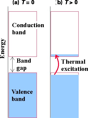
The bands of orbitals arising in any solid lattice provide the orbitals that are available to be occupied by the number of electrons in the crystal. Systems whose highest energy occupied band is completely filled and for which the gap in energy to the lowest unfilled band is large are called insulators because they have no way to easily (i.e., with little energy requirement) promote some of their higher-energy electrons from orbital to orbital and thus effect conduction. The case of diamond discussed above is an example of an insulator. If the band gap between a filled band and an unfilled band is small, it may be possible for thermal excitation (i.e., collisions with neighboring atoms or molecules) to cause excitation of electrons from the former to the latter thereby inducing conductive behavior. The band structures of Al and Ag discussed above offer examples of this case. A simple depiction of how thermal excitations can induce conduction is illustrated in Figure 2.7.
Systems whose highest-energy occupied band is partially filled are also conductors because they have little spacing among their occupied and unoccupied orbitals so electrons can flow easily from one to another. Al and Ag are good examples.
To form a semiconductor, one starts with an insulator whose lower band is filled and whose upper band is empty as shown by the broad bands in Fig.2.8.
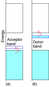
If this insulator material is synthesized with a small amount of “dopant” whose valence orbitals have energies between the filled and empty bands of the insulator, one can generate a semiconductor. If the dopant species has no valence electrons (i.e., has an empty valence orbital), it gives rise to an empty band lying between the filled and empty bands of the insulator as shown below in case a of Figure 2.8. In this case, the dopant band can act as an electron acceptor for electrons excited (either thermally or by light) from the filled band of the insulator into the dopant’s empty band. Once electrons enter the dopant band, charge can flow (because the insulator’s lower band is no longer filled) and the system thus becomes a conductor. Another case is illustrated in the b part of Figure 2.8. Here, the dopant has a filled band that lies close in energy to the empty band of the insulator. Excitation of electrons from this dopant band to the insulator’s empty band can induce current to flow (because now the insulator’s upper band is no longer empty).
Contributors and Attributions
Jack Simons (Henry Eyring Scientist and Professor of Chemistry, U. Utah) Telluride Schools on Theoretical Chemistry
Integrated by Tomoyuki Hayashi (UC Davis)