
Array Detectors
- Page ID
- 75538

Charge Separation and the Photoelectric Effect
Light with sufficient energy can cause charge separation in a semiconductor, such that an electron is promoted from the ground state to the conduction band. The electron (in the conduction band) and corresponding hole (in the ground state) are both mobile. One can thus sense the total amount of light illuminating a semiconductor in two ways: start out with a reverse-biased p-n junction and use the electrons and holes generated by light to discharge that junction, or have electrodes insulated from the semiconductor and biased in such a way that electrons are stored under one electrode, holes under another. The "light discharge" approach is used in photodiode arrays while the "light charge" approach is used for CMOS arrays, charge-coupled arrays, and charge-injection arrays.
Photodiode Arrays (and why they aren't used for emission spectroscopy)
A typical photodiode array has between 128 and 1024 diodes 25 µm wide, 500 - 2500 µm high. Manufacturing uses either CMOS or NMOS technology (the former developing more rapidly, the latter more mature and with wider dynamic range). Each diode has a capacitance of approximately 20 picofarads, so that at saturation potential of 2.5 volts, the stored charge is 50 picocoulombs or about 3×10⁸ electrons. At room temperature, dark current is about 1 picoampere, so the array must be read out several times per minute, lest dark current dominate the observation. Cooling to -35°C is usually sufficient to adequately suppress such currents. Because one strives to work at the shot noise limit where the noise = square root(the number of particles (photons or electons) observed), a diode array is capable of S/N for a single readout of over 104. We will see shortly that this is a higher S/N than many other detectors can provide. The catch is that a diode array works by filling the potential well in the diodes with electrons, allows the diode to be discharged through exposure to light (and by dark current), and then measuring the amount of charge one must supply to recharge the diode to its initial potential. Thus, one is measuring the difference between two numbers, the number of electrons the diode capacitor is holding at the end of a period of time and the number required to fill the well. Any measurement of small differences between large numbers is difficult to make; the diode array is most precise when measuring deep depletion of the stored charge i.e. large photosignals. This is typical of absorption spectrometers measuring high absorbances. For emission spectrometry, one wants to be able to see weak signals, not just strong ones. As a consequence, diode arrays are used in absorption spectrometers but typically not in Raman, fluorescence, or emission spectrometers.
For details on diode arrays, see the websites of the manufacturers, e.g. Hamamatsu.
Charge Coupled Arrays (and why they are used for emission spectroscopy)
From the x-ray to the mid infrared, the most nearly ideal detectors yet invented by humanity are charge-coupled arrays. They may have, over limited energy ranges, detection quantum efficiencies up to 95%. They may have dynamic ranges from a few hundred to 105. While full use of dynamic range may require very slow extraction of data after an image is detected, low-precision full frame readout can be at 1 kHz. Arrays from 1×1 (1 mm square) to 4096×4096 with 50 µm square pixels have been reported, though the largest moderately affordable detectors are typically 1024×1024 15 µm square pixels.
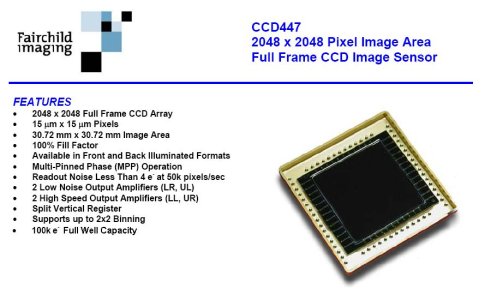
For specifications, see e.g. Fairchild Imaging, Andor Technologies, or Spectral Instruments. Here's a picture of a large format CCD. For the full data sheet and details of how its electronics works, see the data sheet on the web.
If the best characteristics of CCDs were all available in a single unit, one could detect 10 photons striking a single pixel up to several hundred thousand photons on that same pixel. Image intensifiers can be placed in front of CCDs so that, if a single photon releases an avalanche of photoelectrons (as happens in a photomultiplier tube), one detects many photons on the CCD, giving (effectively) single photon detection (though reduced dynamic range -- if one incident photon gives a burst of 20 photons on a single CCD pixel and the full well capacity is 2×10⁵ electrons, then only 104 detected photons will saturate the detector). Because CCDs give x-y data arrays, distortion in spectrometers is of limited concern since the curvature of spectral lines can be taken into account via the software.
Charge Injection Arrays (and why they're uncommon)
With an outstanding description of CIDs available elsewhere on the web, it seems superfluous to go into detail here. Suffice to say that in a CID, one can address individual pixels for readout without having to move the charges off the observation area of the chip, as is required for a CCD. One can thus interogate an image many times, allowing weak signals to accumulate in some pixels while reading the value in brightly illuminate pixels. The accumulated charge in a pixel can then be dumped into the semiconductor substrate (injected -- that's the source of the device name) and integration restarted. This sounds like a terrific way to enhance dynamic range, and it is except for one problem: the single readout noise level is higher than for a CCD. Thus, rapid readout of low intensity signals is not possible. Together with patent restrictions on the device, this means that only a few emission instruments use CIDs. Apparently, a hybrid device with rapid readout and adjustable dynamic range is found in the instruments made by Teledyne Leeman Labs.
CMOS Arrays (and why they'll conquer the world -- eventually)
The most developed process for making integrated circuits is that used to make Complementary Metal Oxide on Silicon (CMOS) devices. The detector chips used in cell phones and inexpensive electronic cameras now use CMOS devices. As of this writing, CMOS does not have the dynamic range of a CCD, and certainly not the outstanding low light level performance. However, some time before 2020, it is likely that the situation will change.