
7.5: Radiation Transducers
- Page ID
- 220456
Radiation Transducers
Simply described, a radiation transducer converts an optical signal, light, into an electrical signal, current or voltage. Quality characteristics instrument makers consider when designing instruments for absorption or emission spectroscopy include:
- The sensitivity
- The signal to noise ratio
- The temporal response response
- The response of the transducer as a function wavelengths
- The signal coming from the transducer in the absence of light (dark current)
- The response of the transducer to different intensities of light (linear or not ?)
A common metric for sensitivity is D* or D-star. D* tells you a detector’s sensitivity for a fixed active detector area (because not all detectors are the same size) and at a specific optical wavelength (because detectors respond differently according to the nature of the incident radiation). The formal definition of D* is the square root of the active area (A, in cm2) divided by the noise equivalent power (NEP) where the NEP is intensity of light that would produce the same amount of signal as the inherent electrical noise coming from the transducer. A sensitive transducer would have a large D* and a low NEP.
The Vacuum Phototube
The vacuum phototube is a small, low cost, optical transducer that works is based on the photoelectric effect. As shown in Figure 7.5.1, a vacuum phototube consists of a large area photocathode with an anode contained in an evacuated quartz envelope. As shown in the circuit in Figure 7.5.2 the photocathode is biased -V and the anode -V by 50 to 90 V. Photons of sufficient energy strike the photocathode surface releasing photoelectrons that are repelled by the cathode and collected at the anode. The current produced is proportional to the intensity of the light. The wavelength response of the vacuum phototube depends on the material coating the photocathode.
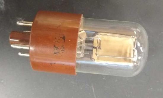
Figure \(\PageIndex {1}\): A photograph of a vacuum phototube.
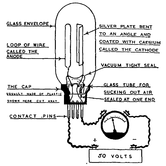
Figure \(\PageIndex {2}\): This old image from the 1954 Bulletin on Narcotics from United Nations Office on Drugs and Crime shows how a vacuum phototube is biased for the collection of photoelectron current.
Coatings fall into one of four categories: (1) highly sensitive, (2) red sensitive, (3) UV sensitive, and (4) flat response . The most sensitive coatings work well in the UV and visible regions are of the bialkali type composed of K, Cs or Sb. A Ga/As (128) coating offers a relatively flat wavelength response for wavelengths 200 - 900 nm. Red sensitive coatings are multi-alkali types such as Na/K/Cs/Sb or Ag/O/CS (S-11) while coatings such as Ga/In/As (S-12) extends the response to 1100 nm but with a loss of sensitivity.
The Photomultiplier Tube
The photomultipler is also based on the photoelectric effect and the same photoemissive surface coating described for the vacuum phototube are also found in photomultiplier tubes. As shown in Figure 7.5.3, the big difference between the phototube and the photomultiplier tube is the series of dynodes between the cathode and anode, all of which are contained in an evacuated quartz envelope. When a photon of sufficient energy strikes the photocathode surface the resulting photoelectron is accelerated towards the first dynode. When the electron strikes the dynode it produces 2 - 3 secondary electrons each of which is accelerated towards the second dynode where they each create 2 - 3 secondary electrons. Figure 7.5.4 shows the potential bias arrangemtns for the photocathod, dynaodes and anode that ensures photoelectrons produced at the cathode are directed towards the anode. For a photomultiplier tube with 9 dynodes, 106 to 107 electrons are produced and collected at the anode for each incident photon. The gain is the number of electrons produced per incident photon.
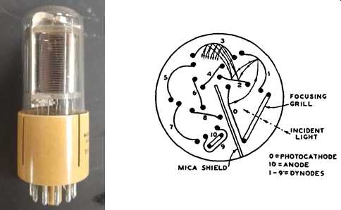
Figure \(\PageIndex {3}\): A photograph of a small, low cost 1p28 photomultipler tube manufactured by the RCA Corp and diagram of the photocathode and dynode structure contained within.
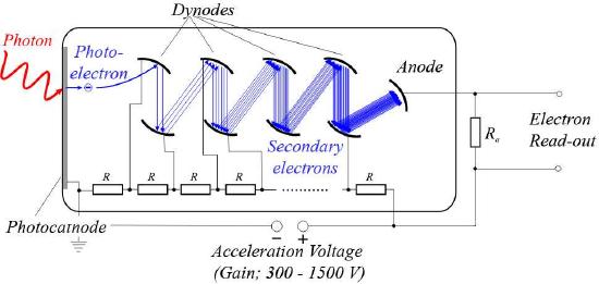
Figure \(\PageIndex {4}\): A sketch illustrating the gain in electrons following creation of the first photelectron in a photomultiplier tube. Image taken from the physicsopenlab.org
Photomultiplier tubes are among the most sensitive and fast optical transducers for UV and visible light. The sensitivity is limited by the dark-current emission the main source of which is thermal emission. Consequently the sensitivity can be improved if need by cooling. Photomultiplier tubes are limited to measuring low-power radiation because intense light can permanently damage the photocathode.
The Silicon Photodiode
The silicon photodiode is a small, rugged and low cost optical transducer that works well over the range of 200 - 1200 nm with a D* better than a vacuum phototube but four orders of magnitude smaller than a photomultiplier tube. As shown in Figure 7.5.5a the diode is reverse biased so that the nominal dark current is small. As illustrated in Figure 7.5.5b, when a light of sufficient energy strikes the p-n junction a new charge pair is generated and the movement of the carrier and holes is measured as a current. The current produced is proportional to the number of photons striking the active region. In Figure 7.5.5c is a photograph of a single photodiode.
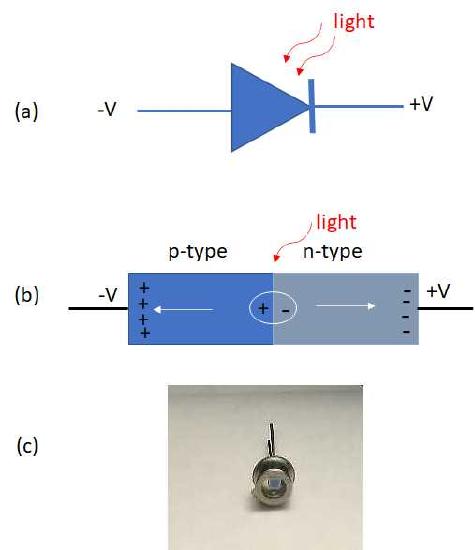
Figure \(\PageIndex {5}\): (a) the voltage arrangement for reversing biasing a photodiode, (b) an illustration of the direction of movement of a new charge pair producing a photocurrent and (c) a photodiode.
Photodiode Arrays
A photodiode array (PDA) is a linear series of small individual silicon photodiodes each one reverse biased and part of a larger integrated circuit. Each individual diode is abut 2.5 mm by 0.025 mm in size and the arrays typically consist of 64 to 4096 diodes. An old PDA with 64 elements is shown in Figure 7.5.6. The most common PDAs have 1024 diodes in a package with a dimension of 2.5 cm. The integrated circuit contains storage capacitors for each photodiode and a circuit for sequentially reading the charge stored for each photodiode. When coupled with a wavelength dispersing device, such as a optical grating, a PDA allows for recording a nm resolution absorption spectrum in a single measurement without the need to scan the wavelength range (change the angle for the grating).
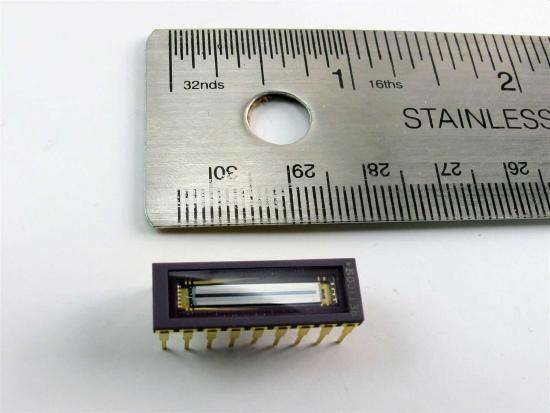
Figure \(\PageIndex {6}\): A 64 element photdiode array manufactured by the EG&G Corp.
Charge - Transfer Devices
Charger- transfer devices, charge injection devices (CIDs) or charge coupled devices (CCDs) are two dimensional arrays of small solid state phototransducers. The D* for these devices is far superior to silicon diode based PDAs and rivals that of photomultiplier tubes . In concept these devices are similar to the camera element in your smartphone although the CMOS technology in your cell phone is superior in terms of low power consumption.
As shown in Figure 7.5.6, when light strikes the active region of a charge transfer device an new charge pair is generated. In a CID the positive holes are collected in a potential well in n-type material created by a negatively biased electrode while in a CCD the electrons are collected in a potential well p-type material created by a positively biased electrode. Each charge collection point is a pixel and today a 1 cm x 1 cm CCD will have at least 1 million pixels.
For both CIDs and CCDs, an integrated circuit allows for a sequential read of the charge stored in each pixel by moving the charge packet within the main silicon substrate by adjusting the potential of the electrodes for each pixel. CID's can be read in a non destructive mode so that the information stored can be read while integration continues. CCD's are more sensitive to low light levels but the readout is destructive of the information.
![]()
Figure \(\PageIndex {7}\): An sketch of a single pixel of a CCD shown the creation of photoelectrons and their capture in a potential well within the main p-type silicon substrate by the potential on the gate electrode.