
10.7: Diodes, LEDs and Solar Cells
- Page ID
- 183358

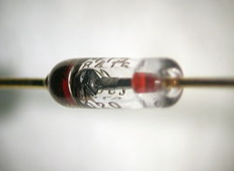
Diodes are semiconductor devices that allow current to flow in only one direction. Diodes act as rectifiers in electronic circuits, and also as efficient light emitters (in LEDs) and solar cells (in photovoltaics). The basic structure of a diode is a junction between a p-type and an n-type semiconductor, called a p-n junction. Typically, diodes are made from a single semiconductor crystal into which p- and n- dopants are introduced.
|
Closeup of a diode, showing the square-shaped semiconductor crystal (black object on left) (John Maushammer, Wikipedia, CC-BY-SA) |
If the n-side of a diode is biased at positive potential and the p-side is biased negative, electrons are drawn to the n-side and holes to the p-side. This reinforces the built in potential of the p-n junction, the width of the depletion layer increases, and very little current flows. This polarization direction is referred to as "back bias." If the diode is biased the other way, carriers are driven into the junction where they recombine. The electric field is diminished, the bands are flattened, and current flows easily since the applied bias lowers the built-in potential. This is called "forward bias."
|
Electrons (red) and holes (white) in a forward-biased diode. (S-kei. Wikipedia, CC-BY-SA) |
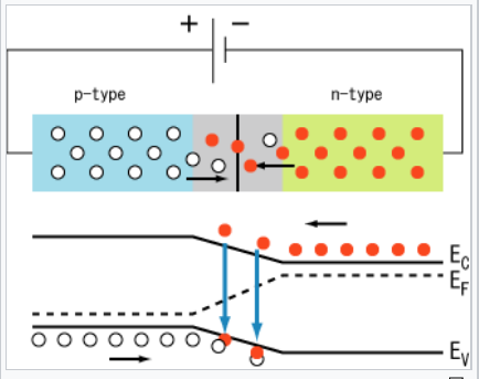
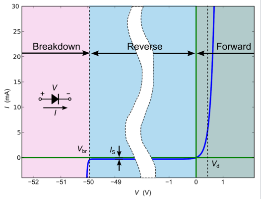
The figure on the left illustrates a forward-biased diode, through which current flows easily. As electrons and holes are driven into the junction (black arrows in lower left figure), they recombine (downward blue arrows), producing light and/or heat. The Fermi level in the diode is indicated as the dotted line. There is a drop in the Fermi level (equal to the applied bias) across the depletion layer. The corresponding diode i-V curve is shown on the right. The current rises exponentially with applied voltage in the forward bias direction, and there is very little leakage current under reverse bias. At very high reverse bias (typically tens of volts) diodes undergo avalanche breakdown and a large reverse current flows.
|
Diode i-V curve |
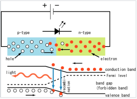
A light-emitting diode or LED is a kind of diode that converts some of the energy of electron-hole recombination into light. This radiative recombination process always occurs in competition with non-radiative recombination, in which the energy is simply converted to heat. When light is emitted from an LED, the photon energy is equal to the bandgap energy. Because of this, LED lights have pure colors and narrow emission spectra relative to other light sources, such as incandescent and fluorescent lights. LED lights are energy-efficient and thus are typically cool to the touch.
|
Light-emitting diode (LED). (S-kei. Wikipedia, CC-BY-SA) |
Direct-gap semiconductors such as GaAs and GaP have efficient luminescence and are also good light absorbers. In direct gap semiconductors, there is no momentum change involved in electron-hole creation or recombination. That is, the electrons and holes originate at the same value of the momentum wavevector k, which we encountered in Ch. 6. k is related to the momentum (also a vector quantity) by p = hk/2π. In a direct-gap semiconductor, the top of the valence band and the bottom of the conduction band most typically both occur at k = 0. Since the momentum of the photon is close to zero, photon absorption and emission are strongly allowed (and thus kinetically fast). Polar semiconductors such as GaAs, GaN, and CdSe are typically direct-gap materials. Indirect-gap semiconductors such as Si and Ge absorb and emit light very weakly because the valence band maximum and conduction band minimum do not occur at the same point in k-space. This means that a lattice vibration (a phonon) must also be created or annihilated in order to conserve momentum. Since this "three body" (electron, hole, phonon) process has low probability, the radiative recombination of electrons and holes is slow relative to non-radiative decay - the thermalization of electron-hole energy as lattice vibrations - in indirect-gap semiconductors. The momentum selection rule thus prevents light absorption/emission and there are no pure Si LEDs or Si-based lasers.
|
Prof. Shuji Nakamura holding a blue LED. |
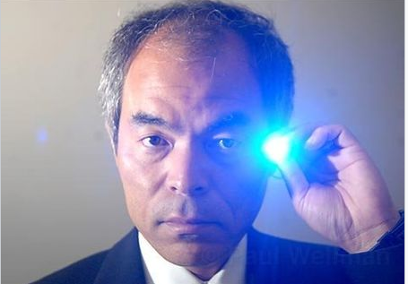
While red, orange, yellow, and green LEDs can be fabricated relatively easily from AlP-GaAs solid solutions, it was initially very difficult to fabricate blue LEDs because the best direct gap semiconductor with a bandgap in the right energy range is a nitride, GaN, which is difficult to make and to dope p-type. Working at Nichia Corporation in Japan, Shuji Nakamura succeeded in developing a manufacturable process for p-GaN, which is the basis of the blue LED. Because of the importance of this work in the development of information storage (Blu-Ray technology) and full-spectrum, energy-efficient LED lighting, Nakamura shared the 2014 Nobel Prize in Physics with Isamu Asaki and Hiroshi Amano, both of whom had made earlier contributions to the development of GaN diodes.
A Solar cell, or photovoltaic cell, converts light absorbed in a p-n junction directly to electricity by the photovoltaic effect. Photovoltaics is the field of technology and research related to the development of solar cells for conversion of solar energy to electricity. Sometimes the term solar cell is reserved for devices intended specifically to capture energy from sunlight, whereas the term photovoltaic cell is used when the light source is unspecified.
|
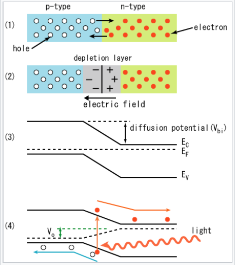
Photovoltaic effect in a semiconductor p-n junction. (S-kei. Wikipedia, CC-BY-SA) |
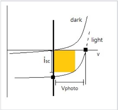
Photocurrent in p-n junction solar cells flows in the diode reverse bias direction. In the dark, the solar cell simply acts as a diode. In the light, the photocurrent can be thought of as a constant current source, which is added to the i-V characteristic of the diode. The relationship between the dark and light current in a photovoltaic cell is shown in the diagram at the left.
|
Current-voltage characteristic of a solar cell in the dark and under illumination with band gap light. The short-circuit photocurrent is indicated as isc, and the open-circuit photovoltage is Vphoto. The maximum power generated by the solar cell is determined by the area of the orange box. |
The built-in electric field of the p-n junction separates e- h+ pairs that are formed by absorption of bandgap light in the depletion region. The electrons flow downhill, towards the n-type side of the junction, the holes flow uphill towards the p-side. If hν ≥ Egap, light can be absorbed by promoting an electron from the valence band to the conduction band. Any excess energy is rapidly thermalized. Light with hν > Eg thus can store only Eg worth of energy in an e- h+ pair. If light is absorbed outside of depletion region, i.e., on the n- or p-side of the junction where there is no electric field, minority carriers must diffuse into the junction in order to be collected. This process occurs in competition with electron-hole recombination. Because impurity atoms and lattice defects make efficient recombination centers, semiconductors used in solar cells (especially indirect-gap materials such as Si, which must be relatively thick in order to absorb most of the solar spectrum) must be very pure. Most of the cost of silicon solar cells is associated with the process of purifying elemental silicon and growing large single crystals from the melt.
In the photodiode i-V curve above, Vphoto is typically only about 70% of the bandgap energy Egap. The photocurrent is limited by the photon flux, the recombination rate, and the re-emission of absorbed light.[6] The area of the orange rectangle indicates the power generated by the solar cell, which can be calculated as P = i x V. In good single crystal or polycrystalline solar cells made of Si, GaAs, CdTe, CuInxGa1-xSe2, or (CH3NH3)PbI3 the quantum yield (the ratio of short circuit photocurrent to photon flux) is close to unity.
|
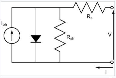
The equivalent circuit of a p-n junction solar cell, which results in the "light" i-V curve shown in the figure above. The solar cell is effectively a diode with a reverse-bias current source provided by light-generated electrons and holes. The shunt resistance (Rsh) in the equivalent circuit represents parasitic electron-hole recombination. A high shunt resistance (low recombination rate) and low series resistance (Rs) are needed for high solar cell efficiency. |
Solar cells have many current applications. Individual cells are used for powering small devices such as electronic calculators. Photovoltaic arrays generate a form of renewable electricity, particularly useful in situations where electrical power from the grid is unavailable such as in remote area power systems, Earth-orbiting satellites and space probes, remote radio-telephones and water pumping applications. Photovoltaic electricity is also increasingly deployed in grid-tied electrical systems.
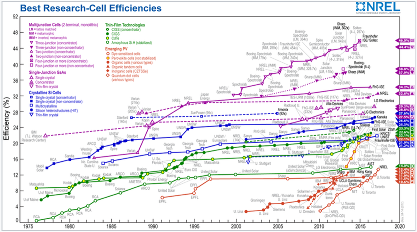
The cost of installed photovoltaics (calculated on a per-watt basis) has dropped over the past decade at a rate of about 13% per year, and has already reached grid parity in Germany and a number of other countries.[7] Photovoltaic grid parity is anticipated in U.S. power markets in the 2020 timeframe.[8] A major driver in the progressively lower cost of photovoltaic power is the steadily increasing efficiency of solar cells, which is shown in the graphic at the right. Higher efficiency solar cells require less area to deliver the same amount of power, and this lowers the "balance of system" costs such as wiring, roof mounting, etc., which scale as the area of the solar panels. Progress towards higher efficiency reflects improved processes for making photovoltaic materials such as silicon and gallium arsenide, as well as the discovery of new materials. Silicon solar cells are a mature technology, so they are now in the flat part of the learning curve and are approaching their maximum theoretical efficiencies. Newer technologies such as organic photovoltaics, quantum dot solar cells, and lead halide perovskite cells are still in the rising part of the learning curve.
|
Reported timeline of solar cell energy conversion efficiencies since 1976 (National Renewable Energy Laboratory) |
A field effect transistor (FET) is a transistor that uses an electric field to control the width of a conducting channel and thus the current in a semiconductor material. It is classified as unipolar transistor, in contrast to bipolar transistors.
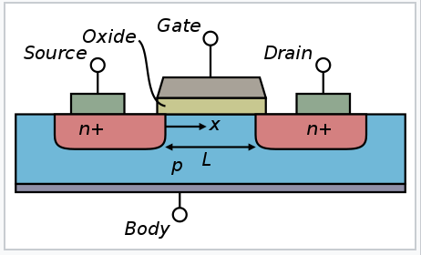
Field effect transistors function as current amplifiers. The typical structure of Si-based FETs is one in which two n-type regions (the source and the drain) are separated by a p-type region. An oxide insulator over the p-type region separates a metal gate lead from the semiconductor. This structure is called a metal-oxide-semiconductor FET (or MOSFET). When voltage is applied between source and drain, current cannot flow because either the n-p or the p-n junction is back-biased. When a positive potential is applied to the gate, however, electrons are driven towards the gate, and locally the semiconductor is "inverted" to n-type. Then the current flows easily between the n-type source and drain through the n-channel. The current flow between the source and drain is many times larger than the current through the gate, and thus the FET can act as an amplifier. Current flow can also represent a logical "1," so FETs are also used in digital logic.
|
Cross section of an n-type MOSFET |
In electronic devices such as microprocessors, field-effect transistors are kept in the off-state most of the time in order to minimize background current and power consumption. The FET shown above, which has n-type source and drain regions, is called an NMOS transistor. In a PMOS transistor, the source and drain regions are p-type and the gate is n-type. In CMOS (complementary metal-oxide semiconductor) integrated circuits, both NMOS and PMOS transistors are used. CMOS circuits are constructed in such a way that all PMOS transistors must have either an input from the voltage source or from another PMOS transistor. Similarly, all NMOS transistors must have either an input from ground or from another NMOS transistor. This arrangement results in low static power consumption.
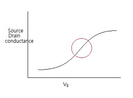
Transistors are most useful in the range of gate voltage (indicated by the red circle in the figure at the left) where the source-drain current changes rapidly. In this region it is possible to effect a large change in current between source and drain when a small signal is applied to the gate. An important figure of merit for FETs is the subthreshold slope, which is the slope a plot of log(current) vs. Vgate. An ideal subthreshold slope is one decade of current per 60 mV of gate bias. Typically, a decade change in source-drain current can be achieved with a change in gate voltage of ~70 mV. The performance of FETs as switches and amplifiers is limited by the subthreshold slope, which in turn is limited by the capacitance of the gate. It is desirable to have a very high gate capacitance, which requires a thin insulating oxide, but also to have a small leakage current, which requires a thick oxide. A current challenge in the semiconductor industry is to continue to scale FETs to even smaller nanoscale dimensions while maintaining acceptable values of these parameters. This is being done by developing new gate insulator materials that have higher dielectric constants than silicon oxide and do not undergo redox reactions with silicon or with metal gate leads. Only a few known materials (such as hafnium oxynitride and hafnium silicates) currently meet these stringent requirements.