
10.10: Problems
- Page ID
- 189590

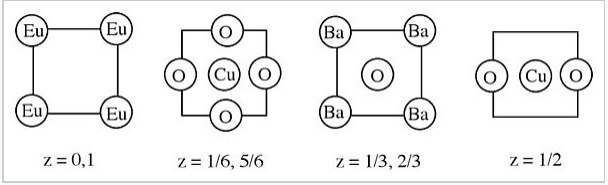
1. The structure of a high temperature superconductor containing barium, europium, copper, and oxygen is shown below. What are the coordination environments of Cu in this compound? This structure is actually closely related to perovskite, ABO3. Explain the relationship between this structure and the ideal perovskite structure.
2. VO2 can exist in insulating or metallic form, depending on temperature and pressure. Which form would be stabilized by increasing the temperature? Explain your answer.
3. Explain briefly how and why the bandgaps for octet p-block semiconductors vary (1) with the average principal quantum number, and (2) with the electronegativity difference between anion and cation.
4. Indicate the type of conduction (n or p) in the following: (a) Se-doped GaAs, (b) InAs1-x, where x << 1, (c) Li0.05Ni0.95O, (d) LixWO3, where x << 1.
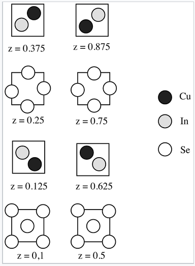
5. The structure of copper indium selenide, a semiconductor used in thin film solar cells, is shown below in sections.
(a) What is the stoichiometry of the compound?
(b) What kind of doping (n or p) will occur if a small amount of iodine is substituted for selenium?
(c) What kind of doping (n or p) will occur if a small fraction of the indium sites are occupied by copper atoms?
6. Using 1 eV = 1240 nm, predict the colors of anatase TiO2 (Eg = 3.1 eV), SiC (2.0 eV), ZnSnP2 (1.7 eV), ZnGeP2 (1.9 eV), and InP (1.27 eV).
7. The conductivity of a certain intrinsic (undoped) semiconductor increases by a factor of two when the temperature is raised from 300 to 330 K. What is the bandgap (in eV)? R = 8.314 J/mol-K, 1 eV/atom = 96.52 kJ/mole.
8. Pure Ge is much more conductive than pure Si. Given their bandgaps (0.74 and 1.15 eV, respectively), estimate the ratio of their conductivities at room temperature.
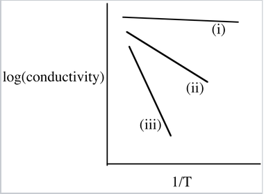
9. The figure below illustrates the trends in conductivity vs. inverse temperature for Si, Ge, and As-doped Ge. Identify lines (i), (ii), and (iii) with the appropriate materials. Explain why the slope of line (i) is close to zero.
10. Sketch a silicon p-n junction, showing the depletion region, band bending, and the Fermi level in the absence of light or applied potential. In the dark, the p-n junction acts as a rectifier. (a) Which way do electrons and holes flow most easily in the dark? (b) Does the built in electric field increase or decrease under forward bias? (c) In the light, the junction acts as a photodiode. In this case, under short circuit conditions, do electrons flow in the same direction or in the opposite direction as in (a)? Explain.