
Scanning Tunneling Microscopy (STM)
- Page ID
- 278428

HOW DOES THE STM WORK?
The STM doesn’t work the way a conventional microscope does, using optics to magnify a sample. Instead a sharp (1-10 nm) probe that is electrically conductive is scanned just above the surface of an electrically conductive sample. The principle of STM is based on tunneling of electrons between this conductive sharp probe and sample.
What is Tunneling?
Tunneling is a phenomenon that describes how electrons flow (or tunnel) across two objects of differing electric potentials when they are brought into close proximity to each other. When a voltage is applied between probe and surface electrons will flow across the gap (probe-sample distance) generating a measurable current.
The tunneling phenomena can be explained by quantum mechanics. Tunneling originates from the wavelike properties of electrons. When two conductors are close enough there is an overlapping of the electron wavefunctions. Electrons can then diffuse across the barrier between the probe (tip-terminating ideally in a single atom) and the sample when a small voltage is applied. The resulting diffusion of electrons is called tunneling. A more detailed quantum mechanics explanation can be found.1
An important characteristic of tunneling is that the amplitude of the current exhibits an exponential decay with the distance, d. One way to describe this relationship is by the equation:
\[\mathrm{I \sim Ve^{–cd}}\nonumber\]
- I = Tunneling current
- V = voltage between probe and sample
- c = constant
- d = probe-sample separation distance
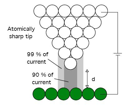
Key factor for STM: Very small changes in the probe-sample separation induce large changes in the tunneling current! (i.e. at a separation of a few Å the current rapidly decreases)
This dependency on tunneling current and probe-sample distance allows for precise control of probe-sample separation, resulting in high vertical resolution(<1 Å) . Furthermore, tunneling is only carried out by the outermost single atom of the probe. This allows for high lateral resolution (<1 Å).
How are the sharp STM probes made?
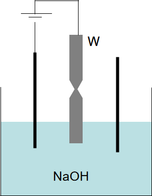
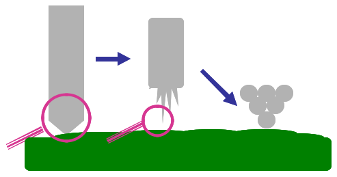
Commercial probes are available but often users make their own probes. A common method is to electrochemically etch tungsten, W, wire in NaOH to create a sharp probe. A problem with W probes is that they oxidize over time. Platinum iridium (Pt-Ir) is preferred for use in air because platinum does not easily oxidize. The tiny fraction of Iridium in the alloy makes it much harder. The Pt-Ir tips are usually shaped by cutting Pt-Ir wire with a wire cutter.
It should be noted that a tip does not necessarily have to be one perfect point.
STM Probe
How does the probe move across the surface?
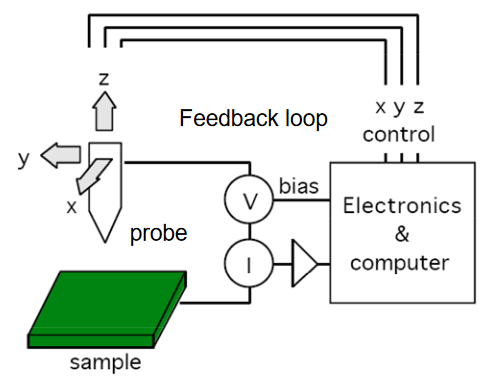
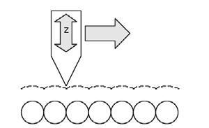
A simple analogy to describe SPM is to think of a stylus of a turntable scanning across a record, Figure 4. However unlike the stylus in a turntable, the probe in SPM does not make direct contact with the surface.

In STM a voltage is applied between the metallic probe and the sample, typically (0-3 V). When the probe is close to the surface (2-4 Å ) the voltage will result in a current, due to tunneling between the probe and sample. When the probe is far away from the surface, the current is zero. The tunneling current produced is low (pA-nA) but can be monitored using amplifiers. A 3D scanner with an electronic feedback loop is used to raster the probe across the sample to obtain a topographical image and monitor the tunneling current.
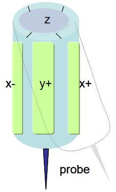
Piezoelectric 3D Scanner
The probe is attached to a 3-D piezoelectric scanner. By adjusting the voltage applied to the scanner the position of the probe can be controlled. This is due to the unique properties of piezoelectric materials that are incorporated into the scanner.
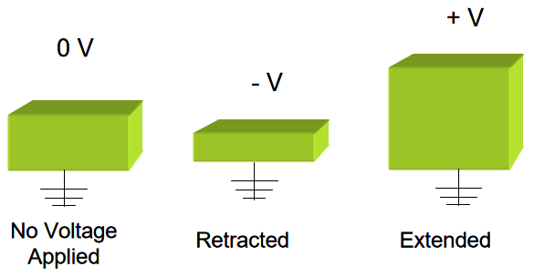
Piezoelectric materials have a permanent dipole moment across unit cell (Example: PbZrTiO3 (PZT)). If the dipoles are oriented, the material changes length in applied electric field. Each scanner responds differently to applied voltage because of the differences in the material properties and dimensions of each piezoelectric element. Sensitivity is a measure of this response, a ratio of how far the piezo extends or contracts per applied volt. A 10-4 to 10-7 % length change per V allows < 1 Å positioning.
Most SPM instruments use a piezoelectric scan tube technology which combines independent piezos to control directions in the x, y, and z. AC voltages applied to the different electrodes produce a scanning (raster) motion in x and y. This motion is controlled by a computer.
- Rastering involves rendering the surface image, pixel by pixel, by sweeping in a vertical and horizontal motion, similar to drawing lines in the dirt with rake.
- The set up described here can also be reversed and the sample can be rastered with piezoelectric scanners underneath the SPM probe.
There are some factors to consider with piezoelectric scanners:
Hysteresis: piezo scanners are more sensitive at the end of travel. Therefore opposite scans will behave differently and display some hysteresis.
Creep: Drift of piezo displacement may occur with large changes in x, y offsets
Aging: Piezoelectric materials' sensitivity to voltages decreases over time. Therefore scanners need to be calibrated on a standard basis
Bow: This is due to the scanner swinging in an arc motion to measure x,y displacement. This is often compensated with the z piezo or by using flattening algorithms.
Imaging Methods
There are two methods of imaging in STM:
1) Constant Current
A constant tunneling current is maintained during scanning (typically 1 nA). This is done by vertically (z) moving the probe at each (x,y) data point until a “setpoint” current is reached. The vertical position of the probe at each (x,y) data point is stored by the computer to form the topographic image of the sample surface. This method is most common in STM.
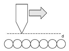
2) Constant Height
In this approach the probe-sample distance is fixed. A variation in tunneling current forms the image. This approaching allows for faster imaging, but only works for flat samples.
Online Interactive Tools
To view an interactive STM model and see how the STM probe moves across a surface you can go to the following website: http://www.iap.tuwien.ac.at/www/_media/surface/stm_gallery/stm_animated.gif
To see how you could possibly build your own STM go here: http://www.e-basteln.de/index_m.htm
WHAT ARE THE LIMITATIONS OF STM?
Although the STM itself does not need vacuum to operate (it works in air as well as under liquids), ultrahigh vacuum (UHV) is required to avoid contamination of the samples from the surrounding medium.
- Complex and expensive instrumentation - especially (UHV) version
- Subject to noise (electrical, vibration)
- Must fabricate probes - dull probes or multiple tips at the end of probe can create serious artifacts
- Only works for conductive samples: metals, semiconductors
- samples can be “altered” to be conductive by coating with Au, but this coating can mask/hide certain features or degrade imaging resolution
References
- For more detail on tunneling and quantum mechanics you can go here: http://www.chembio.uoguelph.ca/educmat/chm729/STMpage/stmdet.htm
- Bonnell, D. A., Ed. Scanning Probe Microscopy and Spectroscopy: Theory, Techniques, and Applications; Wiley-VCH: New York, 2001.