
9.3: SEM and its Applications for Polymer Science
- Page ID
- 55929

SEM and its Applications for Polymer Science
Introduction
The scanning electron microscope (SEM) is a very useful imaging technique that utilized a beam of electrons to acquire high magnification images of specimens. Very similar to the transmission electron microscope (TEM), the SEM maps the reflected electrons and allows imaging of thick (~mm) samples, whereas the TEM requires extremely thin specimens for imaging; however, the SEM has lower magnifications. Although both SEM and TEM use an electron beam, the image is formed very differently and users should be aware of when each microscope is advantageous.
Microscopy Physics
Image Formation
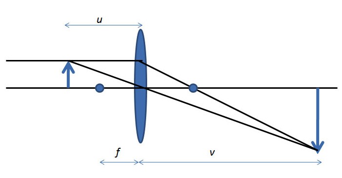
All microscopes serve to enlarge the size of an object and allow people to view smaller regions within the sample. Microscopes form optical images and although instruments like the SEM have extremely high magnifications, the physics of the image formation are very basic. The simplest magnification lens can be seen Figure \(\PageIndex{1}\). The formula for magnification is shown in \ref{1}, where M is magnification, f is focal length, u is the distance between object and lens, and v is distance from lens to the image.
\[ M\ =\ \frac{f}{u-f}\ = \frac{v-f}{f} \label{1} \]
arb.jpg?revision=1)
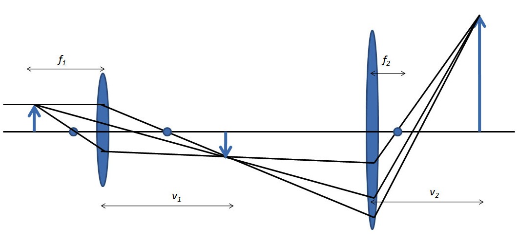
Multistage microscopes can amplify the magnification of the original object even more as shown in Figure. Where magnification is now calculated from \ref{2}, where f1, f2 are focal distances with respect to the first and second lens and v1, v2are the distances from the lens to the magnified image of first and second lens, respectively.
\[M \ =\ \frac{(v_{1}\ -\ f_{1})(v_{2}\ -\ f_{2})}{f_{1}f_{2}} \label{2} \]
arb.jpg?revision=1)
In reality, the objects we wish to magnify need to be illuminated. Whether or not the sample is thin enough to transmit light divides the microscope into two arenas. SEM is used for samples that do not transmit light, whereas the TEM (transmission electron microscope) requires transparent samples. Due to the many frequencies of light from the introduced source, a condenser system is added to control the brightness and narrow the range of viewing to reduce aberrations, which distort the magnified image.
Electron Microscopes
Microscope images can be formed instantaneous (as in the optical microscope or TEM) or by rastering (scanning) a beam across the sample and forming the image point-by-point. The latter is how SEM images are formed. It is important to understand the basic principles behind SEM that define properties and limitations of the image.
Resolution
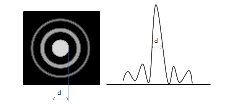
The resolution of a microscope is defined as the smallest distance between two features that can be uniquely identified (also called resolving power). There are many limits to the maximum resolution of the SEM and other microscopes, such as imperfect lenses and diffraction effects. Each single beam of light, once passed through a lens, forms a series of cones called an airy ring (see Figure \(\PageIndex{3}\)). For a given wavelength of light, the central spot size is inversely proportional to the aperture size (i.e., large aperture yields small spot size) and high resolution demands a small spot size.
Aberrations distort the image and we try to minimize the effect as much as possible. Chromatic aberrations are caused by the multiple wavelengths present in white light. Spherical aberrations are formed by focusing inside and outside the ideal focal length and caused by the imperfections within the objective lenses. Astigmatism is because of further distortions in the lens. All aberrations decrease the overall resolution of the microscope.
Electrons
Electrons are charged particles and can interact with air molecules therefore the SEM and TEM instruments require extremely high vacuum to obtain images (10-7 atm). High vacuum ensures that very few air molecules are in the electron beam column. If the electron beam interacts with an air molecule, the air will become ionized and damage the beam filament, which is very costly to repair. The charge of the electron allows scanning and also inherently has a very small deflection angle off the source of the beam.
The electrons are generated with a thermionic filament. A tungsten (W) or LaB6 filament is chosen based on the needs of the user. LaB6 is much more expensive and tungsten filaments meet the needs of the average user. The microscope can be operated as field emission (tungsten filament).
Electron Scattering
To accurately interpret electron microscopy images, the user must be familiar with how high energy electrons can interact with the sample and how these interactions affect the image. The probability that a particular electron will be scattered in a certain way is either described by the cross section, σ, or mean free path, λ, which is the average distance which an electron travels before being scattered.
Elastic Scatter
Elastic scatter, or Rutherford scattering, is defined as a process which deflects an electron but does not decrease its energy. The wavelength of the scattered electron can be detected and is proportional to the atomic number. Elastically scattered electrons have significantly more energy that other types and provide mass contrast imaging. The mean free path, λ, is larger for smaller atoms meaning that the electron travels farther.
Inelastic Scatter
Any process that causes the incoming electron to lose a detectable amount of energy is considered inelastic scattering. The two most common types of inelastic scatter are phonon scattering and plasmon scattering. Phonon scattering occurs when a primary electron looses energy by exciting a phonon, atomic vibrations in a solid, and heats the sample a small amount. A Plasmon is an oscillation within the bulk electrons in the conduction band for metals. Plasmon scattering occurs when an electron interacts with the sample and produces plasmons, which typically have 5 - 30 eV energy loss and small λ.
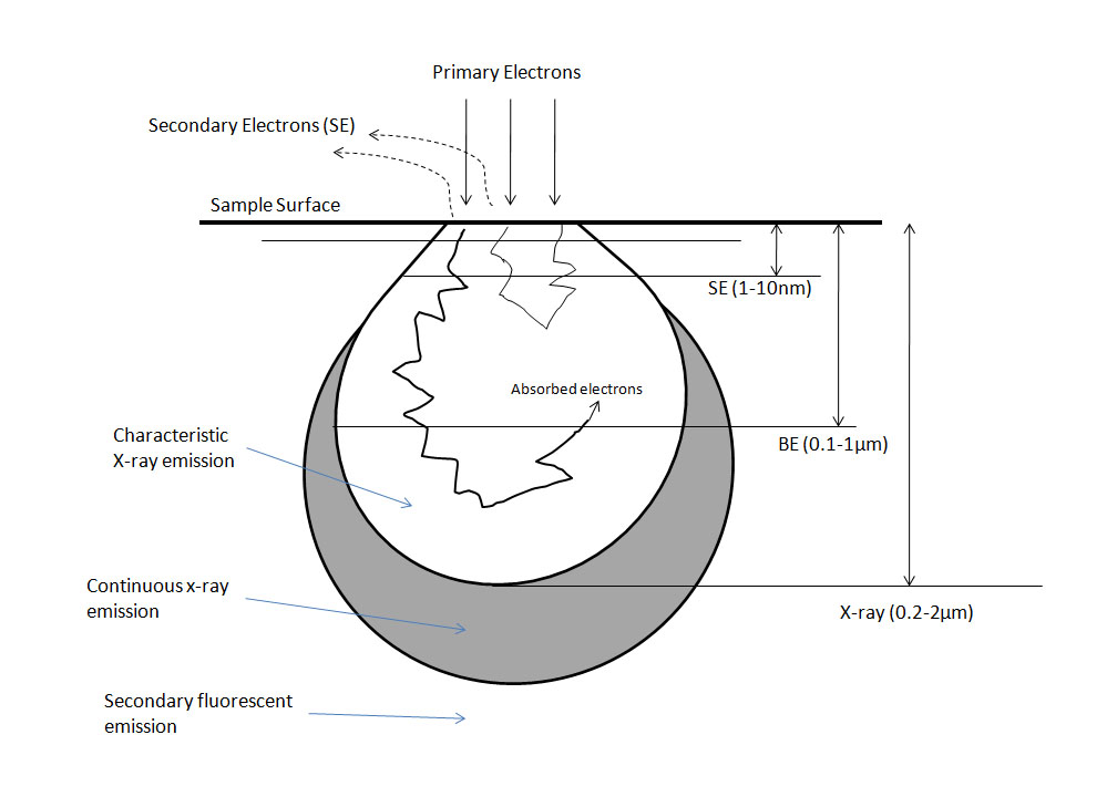
Secondary Effects
A secondary effect is a term describing any event which may be detected outside the specimen and is essentially how images are formed. To form an image, the electron must interact with the sample in one of the aforementioned ways and escape from the sample and be detected. Secondary electrons (SE) are the most common electrons used for imaging due to high abundance and are defined, rather arbitrarily, as electrons with less than 50 eV energy after exiting the sample. Backscattered electrons (BSE) leave the sample quickly and retain a high amount of energy; however there is a much lower yield of BSE. Backscattered electrons are used in many different imaging modes. Refer to Figure \(\PageIndex{4}\) for a diagram of interaction depths corresponding to various electron interactions.
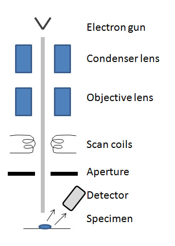
SEM Construction
The SEM is made of several main components: electron gun, condenser lens, scan coils, detectors, specimen, and lenses (see Figure \(\PageIndex{5}\)). Today, portable SEMs are available but the typical size is about 6 feet tall and contains the microscope column and the control console.
A special feature of the SEM and TEM is known as depth of focus, dv/du the range of positions (depths) at which the image can be viewed with good focus, see \ref{3}. This allows the user to see more than a singular plane of a specified height in focus and essentially allows a range of three dimensional imaging.
\[ \frac{dv}{du}\ =\ \frac{-v^{2}}{u^{2}}\ =\ -M^{2} \label{3} \]
Electron Detectors (image formation)
The secondary electron detector (SED) is the main source of SEM images since a large majority of the electrons emitted from the sample are less than 50 eV. These electrons form textural images but cannot determine composition. The SEM may also be equipped with a backscatter electron detector (BSED) which collects the higher energy BSE’s. Backscattered electrons are very sensitive to atomic number and can determine qualitative information about nuclei present (i.e., how much Fe is in the sample). Topographic images are taken by tilting the specimen 20 - 40° toward the detector. With the sample tilted, electrons are more likely to scatter off the top of the sample rather than interact within it, thus yielding information about the surface.
Sample Preparation
The most effective SEM sample will be at least as thick as the interaction volume; depending on the image technique you are using (typically at least 2 µm). For the best contrast, the sample must be conductive or the sample can be sputter-coated with a metal (such as Au, Pt, W, and Ti). Metals and other materials that are naturally conductive do not need to be coated and need very little sample preparation.
SEM of Polymers
As previously discussed, to view features that are smaller than the wavelength of light, an electron microscope must be used. The electron beam requires extremely high vacuum to protect the filament and electrons must be able to adequately interact with the sample. Polymers are typically long chains of repeating units composed primarily of “lighter” (low atomic number) elements such as carbon, hydrogen, nitrogen, and oxygen. These lighter elements have fewer interactions with the electron beam which yields poor contrast, so often times a stain or coating is required to view polymer samples. SEM imaging requires a conductive surface, so a large majority of polymer samples are sputter coated with metals, such as gold.
The decision to view a polymer sample with an SEM (versus a TEM for example) should be evaluated based on the feature size you expect the sample to have. Generally, if you expect the polymer sample to have features, or even individual molecules, over 100 nm in size you can safely choose SEM to view your sample. For much smaller features, the TEM may yield better results, but requires much different sample preparation than will be described here.
Polymer Sample Preparation Techniques
Sputter Coating
A sputter coater may be purchased that deposits single layers of gold, gold-palladium, tungsten, chromium, platinum, titanium, or other metals in a very controlled thickness pattern. It is possible, and desirable, to coat only a few nm’s of metal onto the sample surface.
Spin Coating
Many polymer films are depositing via a spin coater which spins a substrate (often ITO glass) and drops of polymer liquid are dispersed an even thickness on top of the substrate.
Staining
Another option for polymer sample preparation is staining the sample. Stains act in different ways, but typical stains for polymers are osmium tetroxide (OsO4), ruthenium tetroxide (RuO4) phosphotungstic acid (H3PW12O40), hydrazine (N2H4), and silver sulfide (Ag2S).
Examples
Comp-block Copolymer (Microstructure of Cast Film)
- Cast polymer film (see Figure \(\PageIndex{6}\)).
- To view interior structure, the film was cut with a microtome or razor blade after the film was frozen in liquid N2 and fractured.
- Stained with RuO4 vapor (after cutting).
- Structure measurements were averaged over a minimum of 25 measurements.
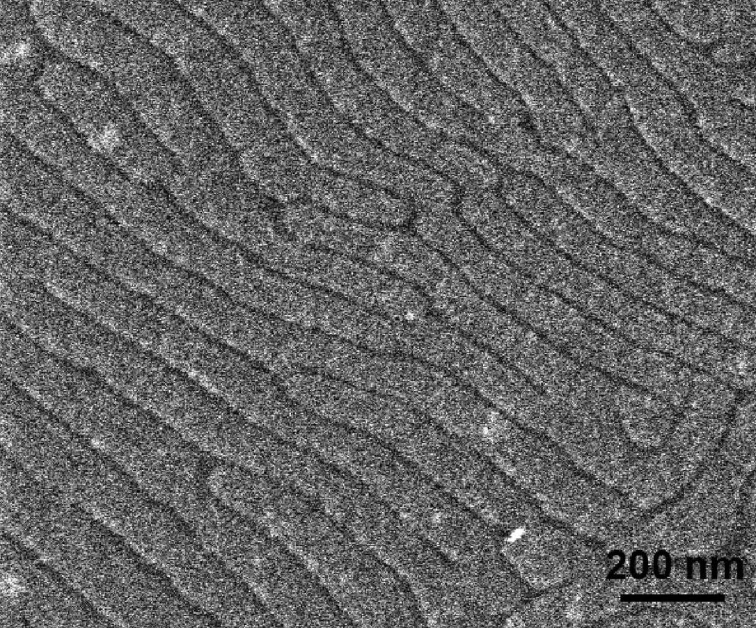
Polystyrene-polylactide Bottlebrush Copolymers (Lamellar Spacing)
- Pressed polymer samples into disks and annealed for 16 h at 170 °C.
- To determine ordered morphologies, the disk was fractured (see Figure \(\PageIndex{7}\)).
- Used SEM to verify lamellar spacing from USAXS.
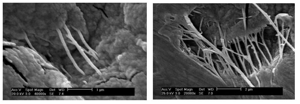
SWNTs in Ultrahigh Molecular Weight Polyethylene
- Dispersed SWNTs in interactive polymer.
- Samples were sputter-coated in gold to enhance contrast.
- The films were solution-crystallized and the cross-section was imaged.
- Environmental SEM (ESEM) was used to show morphologies of composite materials.
- WD = 7 mm.
- Study was conducted to image sample before and after drawing of film.
- Images confirmed the uniform distribution of SWNT in PE (Figure \(\PageIndex{8}\)).
- MW = 10,000 Dalton.
- Study performed to compare transparency before and after UV irradiation.
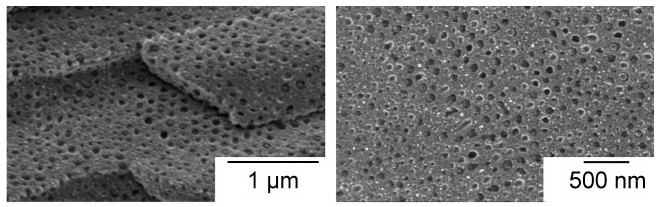
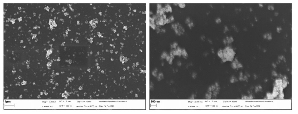
Nanostructures in Conjugated Polymers (Nanoporous Films)
- Polymer and NP were processed into thin films and heated to crosslink.
- SEM was used to characterize morphology and crystalline structure (Figure \(\PageIndex{9}\)).
- SEM was used to determine porosity and pore size.
- Magnified orders of 200 nm - 1 μm.
- WD = 8 mm.
- MW = 23,000 Daltons
- Sample prep: spin coating a solution of poly-(thiophene ester) with copper NPs suspended on to ITO coated glass slides. Ziess, Supra 35
Cryo-SEM Colloid Polystyrene Latex Particles (Fracture Patterns)
- Used cryogenic SEM (cryo-SEM) to visualize the microstructure of particles (Figure \(\PageIndex{10}\))
- Particles were immobilized by fast-freezing in liquid N2 at –196 °C.
- Sample is fractured (-196 °C) to expose cross section.
- 3 nm sputter coated with platinum.
- Shapes of the nanoparticles after fracture were evaluated as a function of crosslink density.
arb.jpg?revision=1)