
7.1: Crystal Structure
- Page ID
- 55904

In any sort of discussion of crystalline materials, it is useful to begin with a discussion of crystallography: the study of the formation, structure, and properties of crystals. A crystal structure is defined as the particular repeating arrangement of atoms (molecules or ions) throughout a crystal. Structure refers to the internal arrangement of particles and not the external appearance of the crystal. However, these are not entirely independent since the external appearance of a crystal is often related to the internal arrangement. For example, crystals of cubic rock salt (NaCl) are physically cubic in appearance. Only a few of the possible crystal structures are of concern with respect to simple inorganic salts and these will be discussed in detail, however, it is important to understand the nomenclature of crystallography.
Crystallography
Bravais Lattice
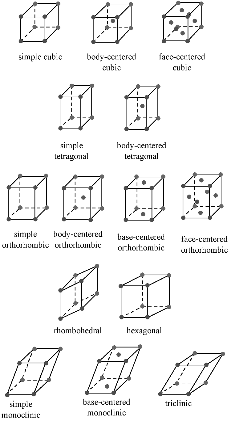
The Bravais lattice is the basic building block from which all crystals can be constructed. The concept originated as a topological problem of finding the number of different ways to arrange points in space where each point would have an identical “atmosphere”. That is each point would be surrounded by an identical set of points as any other point, so that all points would be indistinguishable from each other. Mathematician Auguste Bravais discovered that there were 14 different collections of the groups of points, which are known as Bravais lattices. These lattices fall into seven different "crystal systems”, as differentiated by the relationship between the angles between sides of the “unit cell” and the distance between points in the unit cell. The unit cell is the smallest group of atoms, ions or molecules that, when repeated at regular intervals in three dimensions, will produce the lattice of a crystal system. The “lattice parameter” is the length between two points on the corners of a unit cell. Each of the various lattice parameters are designated by the letters a, b, and c. If two sides are equal, such as in a tetragonal lattice, then the lengths of the two lattice parameters are designated a and c, with b omitted. The angles are designated by the Greek letters α, β, and γsize 12{γ} {}, such that an angle with a specific Greek letter is not subtended by the axis with its Roman equivalent. For example, α is the included angle between the b and c axis.
Table \(\PageIndex{1}\) shows the various crystal systems, while Figure \(\PageIndex{1}\) shows the 14 Bravais lattices. It is important to distinguish the characteristics of each of the individual systems. An example of a material that takes on each of the Bravais lattices is shown in Table \(\PageIndex{2}\).
| System | Axial Lengths and Angles | Unit Cell Geometry |
| cubic | a=b=c, α = β = γ = 90° |  |
| tetragonal | a = b ≠ c, α = β = γ= 90° | 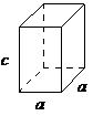 |
| orthorhombic | a ≠ b ≠ c, α = β = γ= 90° | 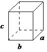 |
| rhombohedral | a = b = c, α = β = γ ≠ 90° | 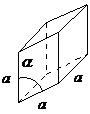 |
| hexagonal | a = b ≠ c, α = β = 90°, γ = 120° | 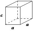 |
| monoclinic | a ≠ b ≠ c, α = γ = 90°, β ≠ 90° | 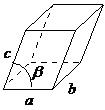 |
| triclinic | a ≠ b ≠ c, α ≠ β ≠ γ | 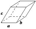 |
| Crystal System | Example |
| triclinic | K2S2O8 |
| monoclinic | As4S4, KNO2 |
| rhombohedral | Hg, Sb |
| hexagonal | Zn, Co, NiAs |
| orthorhombic | Ga, Fe3C |
| tetragonal | In, TiO2 |
| cubic | Au, Si, NaCl |
The cubic lattice is the most symmetrical of the systems. All the angles are equal to 90°, and all the sides are of the same length (a = b = c). Only the length of one of the sides (a) is required to describe this system completely. In addition to simple cubic, the cubic lattice also includes body-centered cubic and face-centered cubic (Figure \(\PageIndex{1}\). Body-centered cubic results from the presence of an atom (or ion) in the center of a cube, in addition to the atoms (ions) positioned at the vertices of the cube. In a similar manner, a face-centered cubic requires, in addition to the atoms (ions) positioned at the vertices of the cube, the presence of atoms (ions) in the center of each of the cubes face.
The tetragonal lattice has all of its angles equal to 90°, and has two out of the three sides of equal length (a = b). The system also includes body-centered tetragonal (Figure \(\PageIndex{1}\).
In an orthorhombic lattice all of the angles are equal to 90°, while all of its sides are of unequal length. The system needs only to be described by three lattice parameters. This system also includes body-centered orthorhombic, base-centered orthorhombic, and face-centered orthorhombic (Figure \(\PageIndex{1}\).
A base-centered lattice has, in addition to the atoms (ions) positioned at the vertices of the orthorhombic lattice, atoms (ions) positioned on just two opposing faces.
The rhombohedral lattice is also known as trigonal, and has no angles equal to 90°, but all sides are of equal length (a = b = c), thus requiring only by one lattice parameter, and all three angles are equal (α = β = γ).
A hexagonal crystal structure has two angles equal to 90°, with the other angle ( γsize 12{γ} {}) equal to 120°. For this to happen, the two sides surrounding the 120° angle must be equal (a = b), while the third side (c) is at 90° to the other sides and can be of any length.
The monoclinic lattice has no sides of equal length, but two of the angles are equal to 90°, with the other angle (usually defined as β) being something other than 90°. It is a tilted parallelogram prism with rectangular bases. This system also includes base-centered monoclinic (Figure \(\PageIndex{2}\)).
In the triclinic lattice none of the sides of the unit cell are equal, and none of the angles within the unit cell are equal to 90°. The triclinic lattice is chosen such that all the internal angles are either acute or obtuse. This crystal system has the lowest symmetry and must be described by 3 lattice parameters (a, b, and c) and the 3 angles (α, β, and γ).
Atom Positions, Crystal Directions and Miller Indices
Atom Positions and Crystal Axes
The structure of a crystal is defined with respect to a unit cell. As the entire crystal consists of repeating unit cells, this definition is sufficient to represent the entire crystal. Within the unit cell, the atomic arrangement is expressed using coordinates. There are two systems of coordinates commonly in use, which can cause some confusion. Both use a corner of the unit cell as their origin. The first, less-commonly seen system is that of Cartesian or orthogonal coordinates (X, Y, Z). These usually have the units of Angstroms and relate to the distance in each direction between the origin of the cell and the atom. These coordinates may be manipulated in the same fashion are used with two- or three-dimensional graphs. It is very simple, therefore, to calculate inter-atomic distances and angles given the Cartesian coordinates of the atoms. Unfortunately, the repeating nature of a crystal cannot be expressed easily using such coordinates. For example, consider a cubic cell of dimension 3.52 Å. Pretend that this cell contains an atom that has the coordinates (1.5, 2.1, 2.4). That is, the atom is 1.5 Å away from the origin in the x direction (which coincides with the a cell axis), 2.1 Å in the y (which coincides with the b cell axis) and 2.4 Å in the z (which coincides with the c cell axis). There will be an equivalent atom in the next unit cell along the x-direction, which will have the coordinates (1.5 + 3.52, 2.1, 2.4) or (5.02, 2.1, 2.4). This was a rather simple calculation, as the cell has very high symmetry and so the cell axes, a, b and c, coincide with the Cartesian axes, X, Y and Z. However, consider lower symmetry cells such as triclinic or monoclinic in which the cell axes are not mutually orthogonal. In such cases, expressing the repeating nature of the crystal is much more difficult to accomplish.
Accordingly, atomic coordinates are usually expressed in terms of fractional coordinates, (x, y, z). This coordinate system is coincident with the cell axes (a, b, c) and relates to the position of the atom in terms of the fraction along each axis. Consider the atom in the cubic cell discussion above. The atom was 1.5 Å in the a direction away from the origin. As the a axis is 3.52 Å long, the atom is (1.5/3.52) or 0.43 of the axis away from the origin. Similarly, it is (2.1/3.52) or 0.60 of the b axis and (2.4/3.5) or 0.68 of the c axis. The fractional coordinates of this atom are, therefore, (0.43, 0.60, 0.68). The coordinates of the equivalent atom in the next cell over in the a direction, however, are easily calculated as this atom is simply 1 unit cell away in a. Thus, all one has to do is add 1 to the x coordinate: (1.43, 0.60, 0.68). Such transformations can be performed regardless of the shape of the unit cell. Fractional coordinates, therefore, are used to retain and manipulate crystal information.
Crystal Directions
The designation of the individual vectors within any given crystal lattice is accomplished by the use of whole number multipliers of the lattice parameter of the point at which the vector exits the unit cell. The vector is indicated by the notation [hkl], where h, k, and l are reciprocals of the point at which the vector exits the unit cell. The origination of all vectors is assumed defined as [000]. For example, the direction along the a-axis according to this scheme would be [100] because this has a component only in the a-direction and no component along either the b or c axial direction. A vector diagonally along the face defined by the a and baxis would be [110], while going from one corner of the unit cell to the opposite corner would be in the [111] direction. Figure \(\PageIndex{2}\) shows some examples of the various directions in the unit cell. The crystal direction notation is made up of the lowest combination of integers and represents unit distances rather than actual distances. A [222] direction is identical to a [111], so [111] is used. Fractions are not used. For example, a vector that intercepts the center of the top face of the unit cell has the coordinates x = 1/2, y = 1/2, z = 1. All have to be inversed to convert to the lowest combination of integers (whole numbers); i.e., [221] in Figure \(\PageIndex{2}\). Finally, all parallel vectors have the same crystal direction, e.g., the four vertical edges of the cell shown in Figure \(\PageIndex{2}\) all have the crystal direction [hkl] = [001].
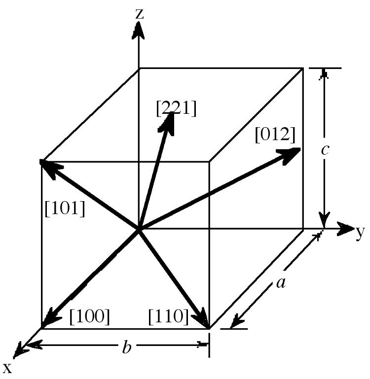
Crystal directions may be grouped in families. To avoid confusion there exists a convention in the choice of brackets surrounding the three numbers to differentiate a crystal direction from a family of direction. For a direction, square brackets [hkl] are used to indicate an individual direction. Angle brackets <hkl> indicate a family of directions. A family of directions includes any directions that are equivalent in length and types of atoms encountered. For example, in a cubic lattice, the [100], [010], and [001] directions all belong to the <100> family of planes because they are equivalent. If the cubic lattice were rotated 90°, the a, b, and cdirections would remain indistinguishable, and there would be no way of telling on which crystallographic positions the atoms are situated, so the family of directions is the same. In a hexagonal crystal, however, this is not the case, so the [100] and [010] would both be <100> directions, but the [001] direction would be distinct. Finally, negative directions are identified with a bar over the negative number instead of a minus sign.
Crystal Planes
Planes in a crystal can be specified using a notation called Miller indices. The Miller index is indicated by the notation [hkl] where h, k, and l are reciprocals of the plane with the x, y, and z axes. To obtain the Miller indices of a given plane requires the following steps:
- The plane in question is placed on a unit cell.
- Its intercepts with each of the crystal axes are then found.
- The reciprocal of the intercepts are taken.
- These are multiplied by a scalar to insure that is in the simple ratio of whole numbers.
For example, the face of a lattice that does not intersect the y or z axis would be (100), while a plane along the body diagonal would be the (111) plane. An illustration of this along with the (111) and (110) planes is given in Figure \(\PageIndex{3}\).
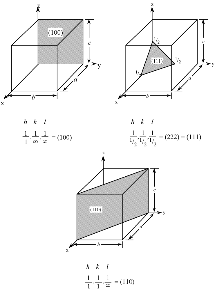
As with crystal directions, Miller indices directions may be grouped in families. Individual Miller indices are given in parentheses (hkl), while braces {hkl} are placed around the indices of a family of planes. For example, (001), (100), and (010) are all in the {100} family of planes, for a cubic lattice.
Description of Crystal Structures
Crystal structures may be described in a number of ways. The most common manner is to refer to the size and shape of the unit cell and the positions of the atoms (or ions) within the cell. However, this information is sometimes insufficient to allow for an understanding of the true structure in three dimensions. Consideration of several unit cells, the arrangement of the atoms with respect to each other, the number of other atoms they in contact with, and the distances to neighboring atoms, often will provide a better understanding. A number of methods are available to describe extended solid-state structures. The most applicable with regard to elemental and compound semiconductor, metals and the majority of insulators is the close packing approach.
Close Packed Structures: Hexagonal Close Packing and Cubic Close Packing
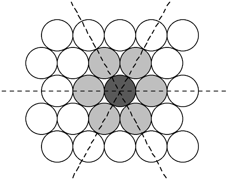
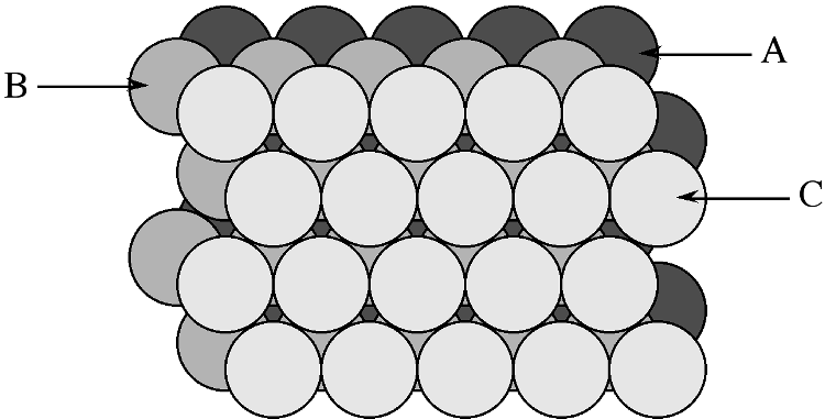
Many crystal structures can be described using the concept of close packing. This concept requires that the atoms (ions) are arranged so as to have the maximum density. In order to understand close packing in three dimensions, the most efficient way for equal sized spheres to be packed in two dimensions must be considered.
The most efficient way for equal sized spheres to be packed in two dimensions is shown in Figure \(\PageIndex{4}\), in which it can be seen that each sphere (the dark gray shaded sphere) is surrounded by, and is in contact with, six other spheres (the light gray spheres in Figure \(\PageIndex{4}\). It should be noted that contact with six other spheres the maximum possible is the spheres are the same size, although lower density packing is possible. Close packed layers are formed by repetition to an infinite sheet. Within these close packed layers, three close packed rows are present, shown by the dashed lines in Figure \(\PageIndex{4}\).
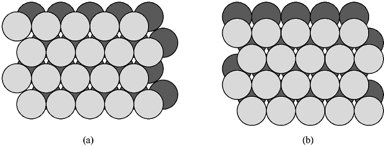
The most efficient way for equal sized spheres to be packed in three dimensions is to stack close packed layers on top of each other to give a close packed structure. There are two simple ways in which this can be done, resulting in either a hexagonal or cubic close packed structures.
Hexagonal Close Packed
If two close packed layers A and B are placed in contact with each other so as to maximize the density, then the spheres of layer B will rest in the hollow (vacancy) between three of the spheres in layer A. This is demonstrated in Figure \(\PageIndex{5}\). Atoms in the second layer, B (shaded light gray), may occupy one of two possible positions (Figure \(\PageIndex{5}\) a or b) but not both together or a mixture of each. If a third layer is placed on top of layer B such that it exactly covers layer A, subsequent placement of layers will result in the following sequence ...ABABAB.... This is known as hexagonal close packing or hcp.
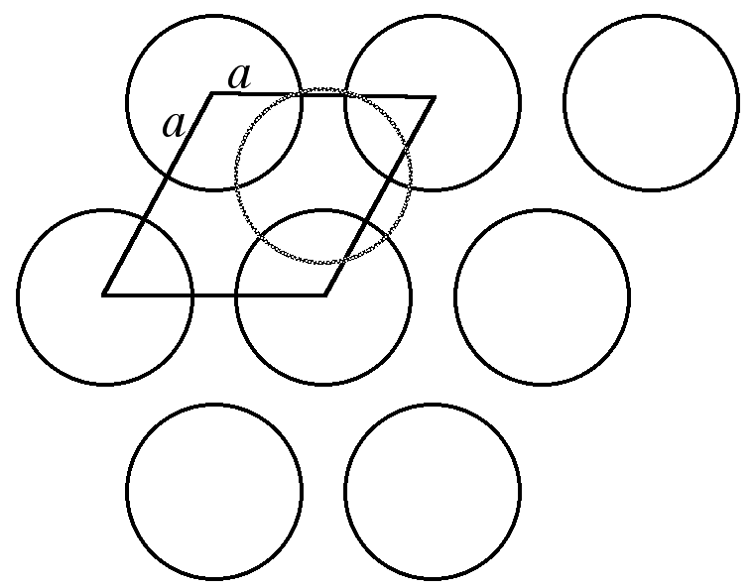
The hexagonal close packed cell is a derivative of the hexagonal Bravais lattice system (Figure \(\PageIndex{6}\) with the addition of an atom inside the unit cell at the coordinates (1/3,2/3,1/2). The basal plane of the unit cell coincides with the close packed layers (Figure \(\PageIndex{6}\). In other words the close packed layer makes-up the {001} family of crystal planes.
The “packing fraction” in a hexagonal close packed cell is 74.05%; that is 74.05% of the total volume is occupied. The packing fraction or density is derived by assuming that each atom is a hard sphere in contact with its nearest neighbors. Determination of the packing fraction is accomplished by calculating the number of whole spheres per unit cell (2 in hcp), the volume occupied by these spheres, and a comparison with the total volume of a unit cell. The number gives an idea of how “open” or filled a structure is. By comparison, the packing fraction for body-centered cubic (Figure \(\PageIndex{5}\)) is 68% and for diamond cubic (an important semiconductor structure to be described later) is it 34%.
Cubic Close Packed: Face-centered Cubic
In a similar manner to the generation of the hexagonal close packed structure, two close packed layers are stacked (Figure \(\PageIndex{7}\) however, the third layer (C) is placed such that it does not exactly cover layer A, while sitting in a set of troughs in layer B (Figure \(\PageIndex{7}\)), then upon repetition the packing sequence will be ...ABCABCABC.... This is known as cubic close packing or ccp.
The unit cell of cubic close packed structure is actually that of a face-centered cubic (fcc) Bravais lattice. In the fcc lattice the close packed layers constitute the {111} planes. As with the hcp lattice packing fraction in a cubic close packed (fcc) cell is 74.05%. Since face centered cubic or fcc is more commonly used in preference to cubic close packed (ccp) in describing the structures, the former will be used throughout this text.
Coordination Number
The coordination number of an atom or ion within an extended structure is defined as the number of nearest neighbor atoms (ions of opposite charge) that are in contact with it. A slightly different definition is often used for atoms within individual molecules: the number of donor atoms associated with the central atom or ion. However, this distinction is rather artificial, and both can be employed.
The coordination numbers for metal atoms in a molecule or complex are commonly 4, 5, and 6, but all values from 2 to 9 are known and a few examples of higher coordination numbers have been reported. In contrast, common coordination numbers in the solid state are 3, 4, 6, 8, and 12. For example, the atom in the center of body-centered cubic lattice has a coordination number of 8, because it touches the eight atoms at the corners of the unit cell, while an atom in a simple cubic structure would have a coordination number of 6. In both fcc and hcp lattices each of the atoms have a coordination number of 12.
Octahedral and Tetrahedral Vacancies
As was mentioned above, the packing fraction in both fcc and hcp cells is 74.05%, leaving 25.95% of the volume unfilled. The unfilled lattice sites (interstices) between the atoms in a cell are called interstitial sites or vacancies. The shape and relative size of these sites is important in controlling the position of additional atoms. In both fcc and hcp cells most of the space within these atoms lies within two different sites known as octahedral sites and tetrahedral sites. The difference between the two lies in their “coordination number”, or the number of atoms surrounding each site. Tetrahedral sites (vacancies) are surrounded by four atoms arranged at the corners of a tetrahedron. Similarly, octahedral sites are surrounded by six atoms which make-up the apices of an octahedron. For a given close packed lattice an octahedral vacancy will be larger than a tetrahedral vacancy.
Within a face centered cubic lattice, the eight tetrahedral sites are positioned within the cell, at the general fractional coordinate of (n/4,n/4,n/4) where n = 1 or 3, e.g., (1/4,1/4,1/4), (1/4,1/4,3/4), etc. The octahedral sites are located at the center of the unit cell (1/2,1/2,1/2), as well as at each of the edges of the cell, e.g., (1/2,0,0). In the hexagonal close packed system, the tetrahedral sites are at (0,0,3/8) and (1/3,2/3,7/8), and the octahedral sites are at (1/3,1/3,1/4) and all symmetry equivalent positions.
Important Structure Types
The majority of crystalline materials do not have a structure that fits into the one atom per site simple Bravais lattice. A number of other important crystal structures are found, however, only a few of these crystal structures are those of which occur for the elemental and compound semiconductors and the majority of these are derived from fcc or hcp lattices. Each structural type is generally defined by an archetype, a material (often a naturally occurring mineral) which has the structure in question and to which all the similar materials are related. With regard to commonly used elemental and compound semiconductors the important structures are diamond, zinc blende, Wurtzite, and to a lesser extent chalcopyrite. However, rock salt, β-tin, cinnabar and cesium chloride are observed as high pressure or high temperature phases and are therefore also discussed. The following provides a summary of these structures. Details of the full range of solid-state structures are given elsewhere.
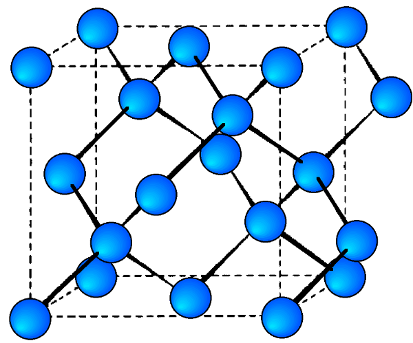
Diamond Cubic
The diamond cubic structure consists of two interpenetrating face-centered cubic lattices, with one offset 1/4 of a cube along the cube diagonal. It may also be described as face centered cubic lattice in which half of the tetrahedral sites are filled while all the octahedral sites remain vacant. The diamond cubic unit cell is shown in Figure \(\PageIndex{8}\). Each of the atoms (e.g., C) is four coordinate, and the shortest interatomic distance (C-C) may be determined from the unit cell parameter (a).
\[ C-C\ =\ a \frac{\sqrt{3} }{4} \approx \ 0.422 a \label{1} \]
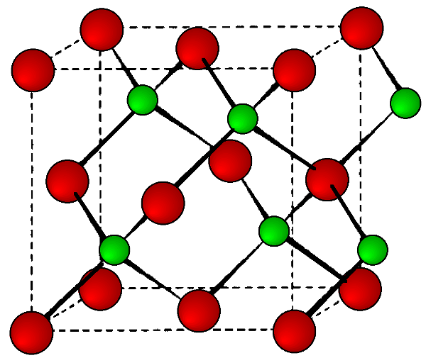
Zinc Blende
This is a binary phase (ME) and is named after its archetype, a common mineral form of zinc sulfide (ZnS). As with the diamond lattice, zinc blende consists of the two interpenetrating fcc lattices. However, in zinc blende one lattice consists of one of the types of atoms (Zn in ZnS), and the other lattice is of the second type of atom (S in ZnS). It may also be described as face centered cubic lattice of S atoms in which half of the tetrahedral sites are filled with Zn atoms. All the atoms in a zinc blende structure are 4-coordinate. The zinc blende unit cell is shown in Figure \(\PageIndex{9}\). A number of inter-atomic distances may be calculated for any material with a zinc blende unit cell using the lattice parameter (a).
\[ Zn-S\ =\ a \frac{\sqrt{3} }{4} \approx \ 0.422 a \label{2} \]
\[ Zn-Zn \ =\ S-S\ = \frac{a}{\sqrt{2}} \approx 0.707\ a \label{3} \]
Chalcopyrite
The mineral chalcopyrite CuFeS2 is the archetype of this structure. The structure is tetragonal (a = b ≠ c, α = β = γ = 90°, and is essentially a superlattice on that of zinc blende. Thus, is easiest to imagine that the chalcopyrite lattice is made-up of a lattice of sulfur atoms in which the tetrahedral sites are filled in layers, ...FeCuCuFe..., etc. (Figure \(\PageIndex{10}\). In such an idealized structure c = 2a, however, this is not true of all materials with chalcopyrite structures.
Rock Salt
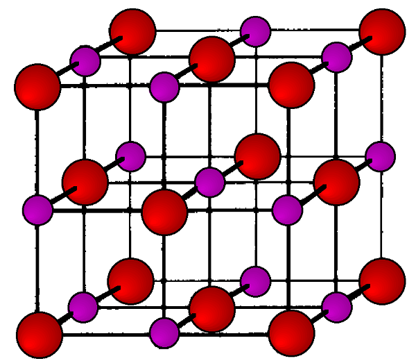
As its name implies the archetypal rock salt structure is NaCl (table salt). In common with the zinc blende structure, rock salt consists of two interpenetrating face-centered cubic lattices. However, the second lattice is offset 1/2a along the unit cell axis. It may also be described as face centered cubic lattice in which all of the octahedral sites are filled, while all the tetrahedral sites remain vacant, and thus each of the atoms in the rock salt structure are 6-coordinate. The rock salt unit cell is shown in Figure \(\PageIndex{11}\). A number of inter-atomic distances may be calculated for any material with a rock salt structure using the lattice parameter (a).
\[ Na-Cl\ =\ \frac{a}{2} \approx 0.5 a \label{4} \]
\[ Na-Na \ =\ Cl-Cl \ =\ \frac{a}{\sqrt{2}} \approx 0.707\ a \label{5} \]
Cinnabar
Cinnabar, named after the archetype mercury sulfide, HgS, is a distorted rock salt structure in which the resulting cell is rhombohedral (trigonal) with each atom having a coordination number of six.
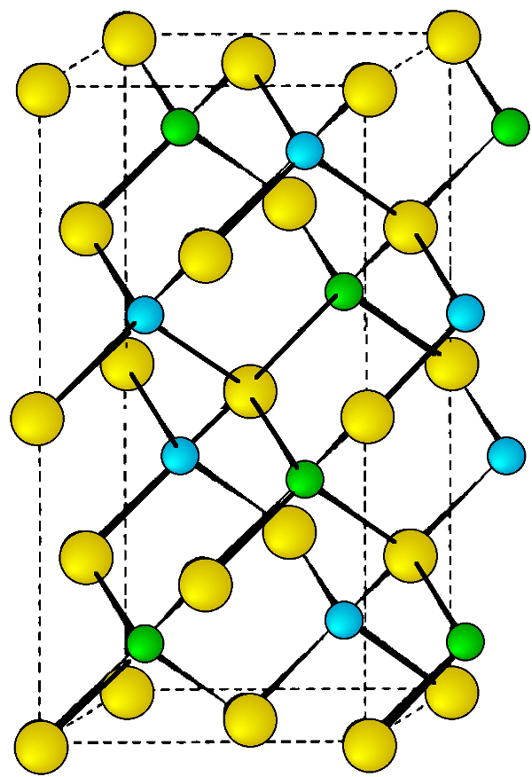
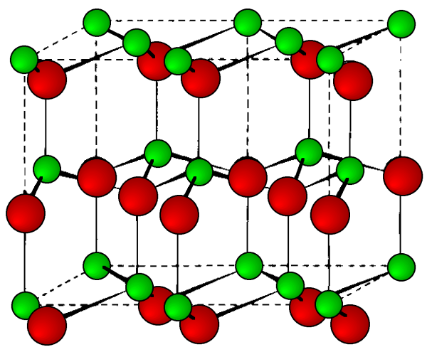
Wurtzite
This is a hexagonal form of the zinc sulfide. It is identical in the number of and types of atoms, but it is built from two interpenetrating hcp lattices as opposed to the fcc lattices in zinc blende. As with zinc blende all the atoms in a wurtzite structure are 4-coordinate. The wurtzite unit cell is shown in Figure \(\PageIndex{12}\). A number of inter atomic distances may be calculated for any material with a wurtzite cell using the lattice parameter (a).
\[ Zn-S\ =\ a \sqrt{3/8 } \ =\ 0.612\ a\ = \frac{3 c}{8} \ =\ 0.375\ c \label{6} \]
\[ Zn- Zn \ =\ S-S\ =\ a\ =\ 1.632\ c \label{7} \]
However, it should be noted that these formulae do not necessarily apply when the ratio a/c is different from the ideal value of 1.632.
Cesium Chloride
The cesium chloride structure is found in materials with large cations and relatively small anions. It has a simple (primitive) cubic cell (Figure \(\PageIndex{13}\)) with a chloride ion at the corners of the cube and the cesium ion at the body center. The coordination numbers of both Cs+ and Cl-, with the inner atomic distances determined from the cell lattice constant (a).
\[ Cs-Cl\ =\ \frac{a \sqrt{3} }{2} \approx 0.866a \label{8} \]
\[Cs-Cs \ =\ Cl-Cl\ = a \label{9} \]
β-Tin
The room temperature allotrope of tin is β-tin or white tin. It has a tetragonal structure, in which each tin atom has four nearest neighbors (Sn-Sn = 3.016 Å) arranged in a very flattened tetrahedron, and two next nearest neighbors (Sn-Sn = 3.175 Å). The overall structure of β-tin consists of fused hexagons, each being linked to its neighbor via a four-membered Sn4 ring.
Defects in Crystalline Solids
Up to this point we have only been concerned with ideal structures for crystalline solids in which each atom occupies a designated point in the crystal lattice. Unfortunately, defects ordinarily exist in equilibrium between the crystal lattice and its environment. These defects are of two general types: point defects and extended defects. As their names imply, point defects are associated with a single crystal lattice site, while extended defects occur over a greater range.
Point Defects: "Too Many or Too Few" or "Just Plain Wrong"
Point defects have a significant effect on the properties of a semiconductor, so it is important to understand the classes of point defects and the characteristics of each type. Figure \(\PageIndex{13}\) summarizes various classes of native point defects, however, they may be divided into two general classes; defects with the wrong number of atoms (deficiency or surplus) and defects where the identity of the atoms is incorrect.
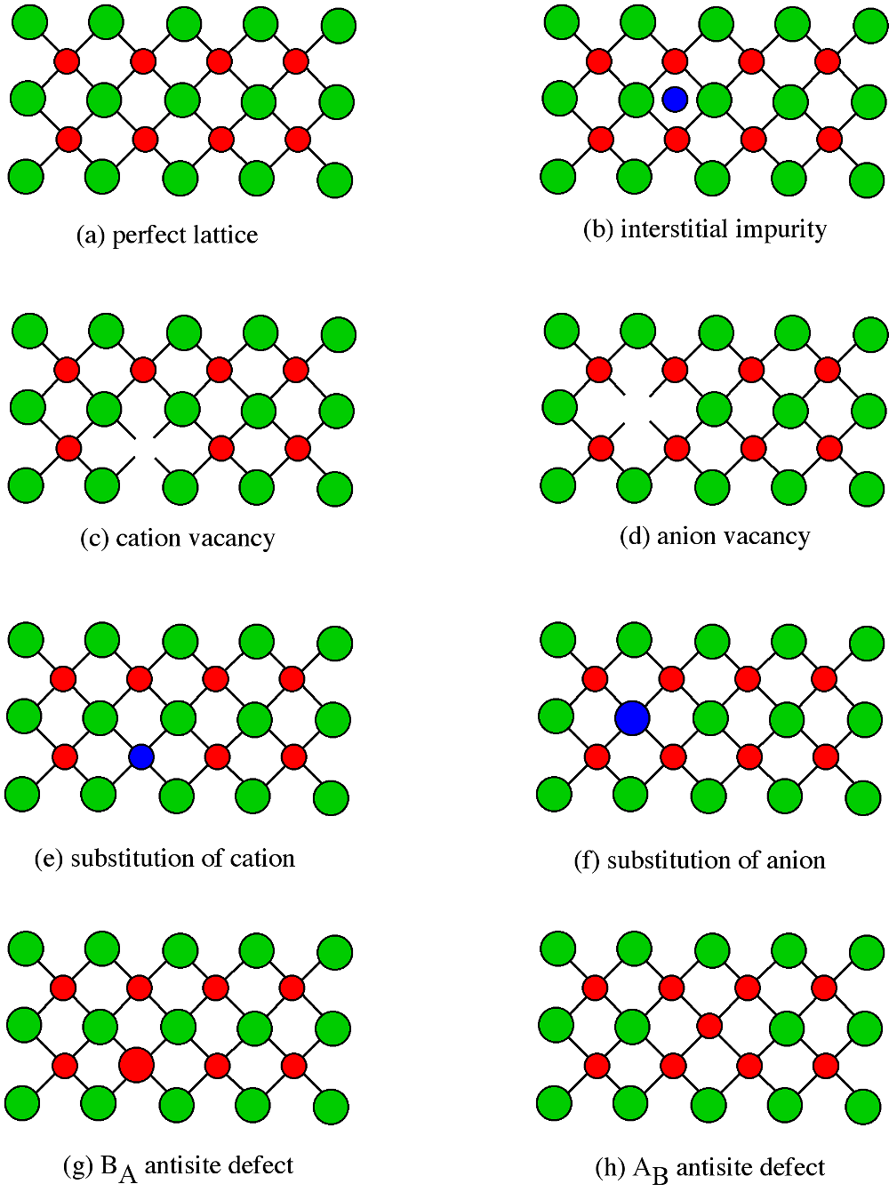
Interstitial Impurity
An interstitial impurity occurs when an extra atom is positioned in a lattice site that should be vacant in an ideal structure (Figure \(\PageIndex{13}\) b).Since all the adjacent lattice sites are filled the additional atom will have to squeeze itself into the interstitial site, resulting in distortion of the lattice and alteration in the local electronic behavior of the structure. Small atoms, such as carbon, will prefer to occupy these interstitial sites. Interstitial impurities readily diffuse through the lattice via interstitial diffusion, which can result in a change of the properties of a material as a function of time. Oxygen impurities in silicon generally are located as interstitials.
Vacancies
The converse of an interstitial impurity is when there are not enough atoms in a particular area of the lattice. These are called vacancies. Vacancies exist in any material above absolute zero and increase in concentration with temperature. In the case of compound semiconductors, vacancies can be either cation vacancies (Figure \(\PageIndex{13}\) c) or anion vacancies (Figure \(\PageIndex{13}\) d), depending on what type of atom are “missing”.
Substitution
Substitution of various atoms into the normal lattice structure is common, and used to change the electronic properties of both compound and elemental semiconductors. Any impurity element that is incorporated during crystal growth can occupy a lattice site. Depending on the impurity, substitution defects can greatly distort the lattice and/or alter the electronic structure. In general, cations will try to occupy cation lattice sites (Figure \(\PageIndex{13}\) e), and anion will occupy the anion site (Figure \(\PageIndex{13}\) f). For example, a zinc impurity in GaAs will occupy a gallium site, if possible, while a sulfur, selenium and tellurium atoms would all try to substitute for an arsenic. Some impurities will occupy either site indiscriminately, e.g., Si and Sn occupy both Ga and As sites in GaAs.
Antisite Defects
Antisite defects are a particular form of substitution defect, and are unique to compound semiconductors. An antisite defect occurs when a cation is misplaced on an anion lattice site or vice versa ( Figure \(\PageIndex{13}\) g and h).Dependant on the arrangement these are designated as either AB antisite defects or BA antisite defects. For example, if an arsenic atom is on a gallium lattice site the defect would be an AsGa defect. Antisite defects involve fitting into a lattice site atoms of a different size than the rest of the lattice, and therefore this often results in a localized distortion of the lattice. In addition, cations and anions will have a different number of electrons in their valence shells, so this substitution will alter the local electron concentration and the electronic properties of this area of the semiconductor.
Extended Defects: Dislocations in a Crystal Lattice
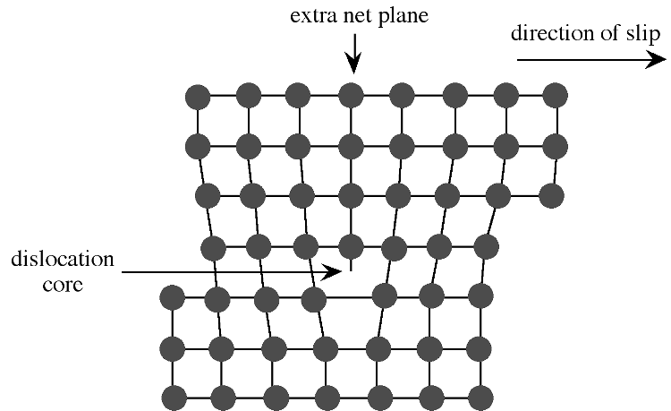
Extended defects may be created either during crystal growth or as a consequence of stress in the crystal lattice. The plastic deformation of crystalline solids does not occur such that all bonds along a plane are broken and reformed simultaneously. Instead, the deformation occurs through a dislocation in the crystal lattice. Figure shows a schematic representation of a dislocation in a crystal lattice. Two features of this type of dislocation are the presence of an extra crystal plane, and a large void at the dislocation core. Impurities tend to segregate to the dislocation core in order to relieve strain from their presence.
Epitaxy
Epitaxy, is a transliteration of two Greek words epi, meaning "upon", and taxis, meaning "ordered". With respect to crystal growth it applies to the process of growing thin crystalline layers on a crystal substrate. In epitaxial growth, there is a precise crystal orientation of the film in relation to the substrate. The growth of epitaxial films can be done by a number of methods including molecular beam epitaxy, atomic layer epitaxy, and chemical vapor deposition, all of which will be described later.
Epitaxy of the same material, such as a gallium arsenide film on a gallium arsenide substrate, is called homoepitaxy, while epitaxy where the film and substrate material are different is called heteroepitaxy. Clearly, in homoepitaxy, the substrate and film will have the identical structure, however, in heteroepitaxy, it is important to employ where possible a substrate with the same structure and similar lattice parameters. For example, zinc selenide (zinc blende, a = 5.668 Å) is readily grown on gallium arsenide (zinc blende, a = 5.653 Å). Alternatively, epitaxial crystal growth can occur where there exists a simple relationship between the structures of the substrate and crystal layer, such as is observed between Al2O3 (100) on Si (100). Whichever route is chosen a close match in the lattice parameters is required, otherwise, the strains induced by the lattice mismatch results in distortion of the film and formation of dislocations. If the mismatch is significant epitaxial growth is not energetically favorable, causing a textured film or polycrystalline untextured film to be grown. As a general rule of thumb, epitaxy can be achieved if the lattice parameters of the two materials are within about 5% of each other. For good quality epitaxy, this should be less than 1%. The larger the mismatch, the larger the strain in the film. As the film gets thicker and thicker, it will try to relieve the strain in the film, which could include the loss of epitaxy of the growth of dislocations. It is important to note that the <100> directions of a film must be parallel to the <100> direction of the substrate. In some cases, such as Fe on MgO, the [111] direction is parallel to the substrate [100]. The epitaxial relationship is specified by giving first the plane in the film that is parallel to the substrate [100].